Electrostatic discharge protection circuit for RF identification chip

A technology of electrostatic discharge protection and radio frequency identification, applied in circuits, electrical components, electric solid devices, etc., can solve problems such as performance degradation, failure to work, passivation layer cracks, etc., and achieve strong ESD resistance and fast turn-on time.

Inactive Publication Date: 2007-04-18
BEIJING CEC HUADA ELECTRONIC DESIGN CO LTD
View PDF0 Cites 5 Cited by
  • Summary
  • Abstract
  • Description
  • Claims
  • Application Information

AI Technical Summary

Problems solved by technology

For CMOS process IC chips, IC failures caused by ESD include reverse breakdown of the PN junction, breakdown of the gate oxide layer and damage to the metal connection line, and cracks in the passivation layer and electromigration damage may a

Method used


Image

  • Electrostatic discharge protection circuit for RF identification chip
  • Electrostatic discharge protection circuit for RF identification chip
  • Electrostatic discharge protection circuit for RF identification chip

Examples


Embodiment Construction

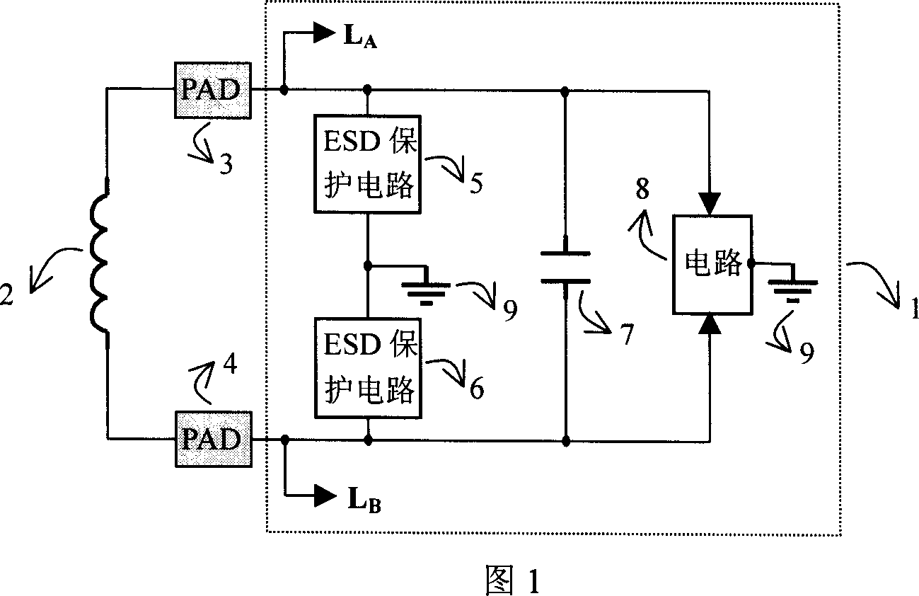
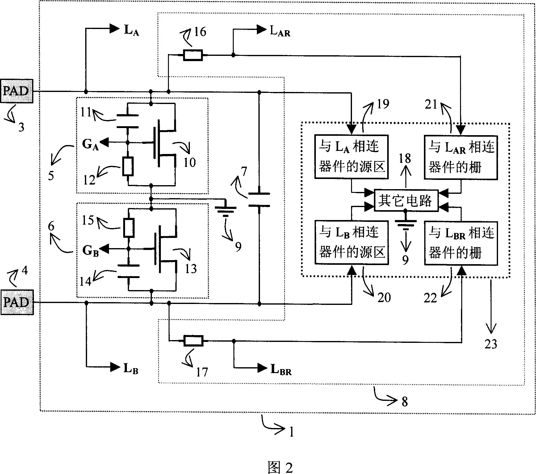
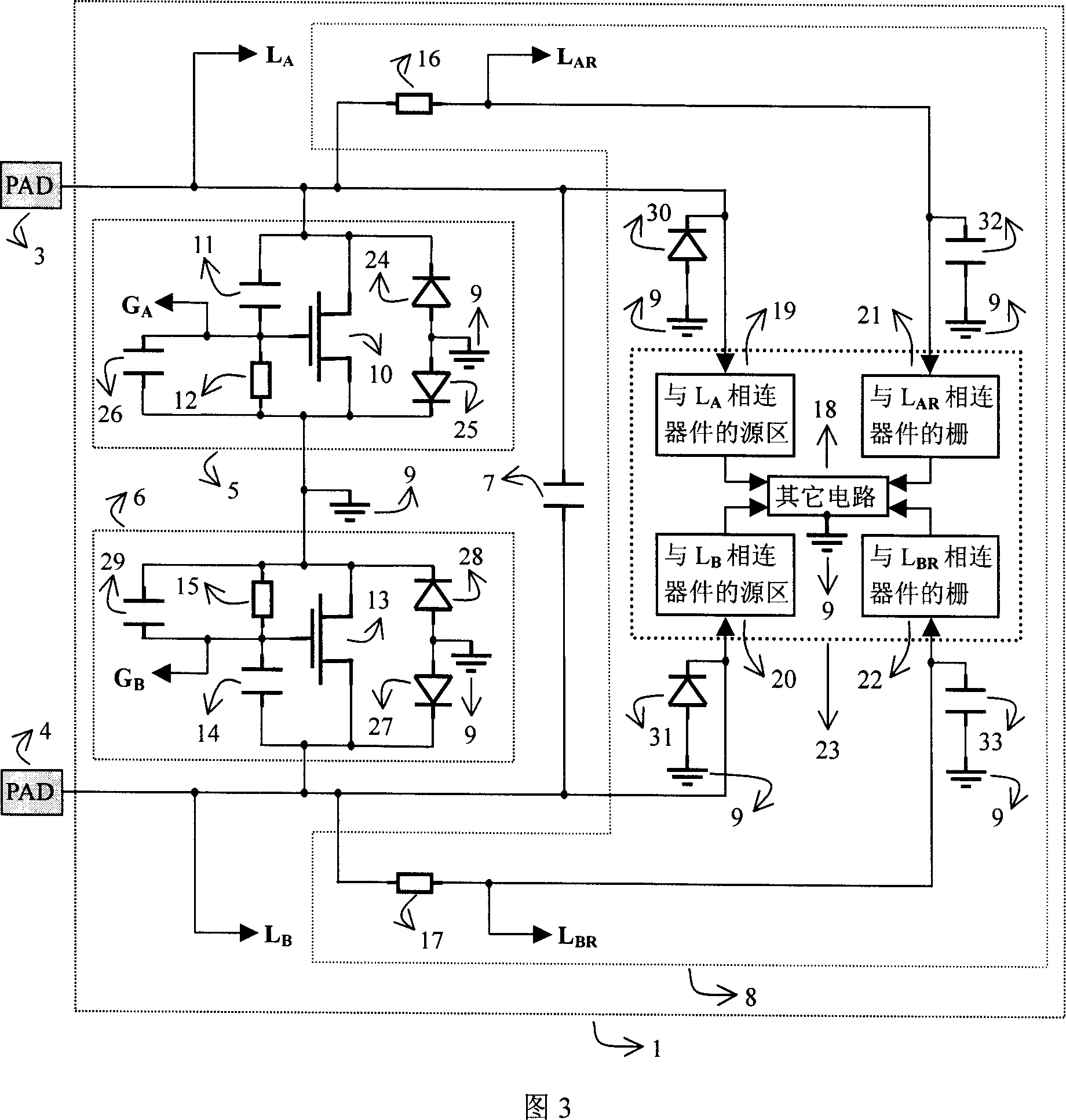
[0018] 5.1 Circuit structure

[0019] The ESD protection circuit structure is shown in Figure 2.

[0020] Among them, the discharge capacity, turn-on time and process insensitivity can be achieved by designing ESD protection circuits 5 and 6. Under the discharge phenomenon that the ESD protection circuit cannot be turned on, the ESD protection circuit and related circuits have certain resistance capabilities by selecting appropriate devices (Including 7, 10-17, 19-22 in the figure) to achieve; ESD protection circuit can not affect the normal operation of the chip to achieve through the overall design of circuit parameters.

[0021] 5.2 Parameter design

[0022] Since L A End and L B End has symmetry, so we only use L A Take the circuit parameter design of the terminal as an example.

[0023] A). Discharge capacity design

[0024] This can be achieved by designing the aspect ratio of the NMOS tube 10 in the ESD protection circuit 5, and the specific layout requires comprehensive co...


PUM


Abstract

The invention advances a CMOS process-based on-chip electrostatic discharge (ESD) protection circuit applied to radio frequency identification (RFID) chips, composed of chip ground on-chip ESD protection circuit used to connect two pressure points of an outside-chip antenna, and inside-chip circuit directly or indirectly connected with pressure points, and giving circuit structure and design method, where the on-chip ESD protection circuit for the RFID chip is an important solution to assure the chip avoids ESD failure. And it considers three discharging models of human body model (HBM), machine model (MM) and charging device model (CDM) and simultaneously considers validity of ESD protection circuit and insensibility to process, and it is an ESD protection circuit with strong robustness, applied to RFID chip.

Description

1. Technical Field [0001] The invention is an on-chip electrostatic discharge protection circuit for radio frequency identification chips, which is characterized by considering the three electrostatic discharge models of HBM, MM and CDM, while ensuring the effectiveness of the electrostatic discharge protection circuit and its insensitivity to the process. In other words, the proposed electrostatic discharge protection circuit for radio frequency identification chips has strong effectiveness and robustness. 2. Background technology [0002] Electrostatic discharge (ESD) phenomenon often occurs in people's daily life, and it is also one of the main reasons for the failure of integrated circuit (IC) chips. For CMOS process IC chips, IC failures caused by ESD include reverse breakdown of PN junction, gate oxide breakdown, and metal connection line damage. Passivation layer cracks and electromigration damage may also occur. When the IC device is in operation, a latch-up effect may al...

Claims


Application Information

Patent Timeline
IPC IPC(8): H01L27/02H01L23/60
Inventor 周建锁潘亮刘华茂叶茵
Owner BEIJING CEC HUADA ELECTRONIC DESIGN CO LTD
Why Eureka
Try Eureka