
Current-controlled cmos wideband amplifier/equalizer circuit

An equalizer circuit and current control technology, applied in amplifiers, improving amplifiers to expand bandwidth, and components of amplifying devices, etc., can solve problems such as reduced impedance matching, different delays, and reduced data path bandwidth.

Active Publication Date: 2007-02-21
AVAGO TECH INT SALES PTE LTD
View PDF5 Cites 14 Cited by
  • Summary
  • Abstract
  • Description
  • Claims
  • Application Information

AI Technical Summary

Problems solved by technology

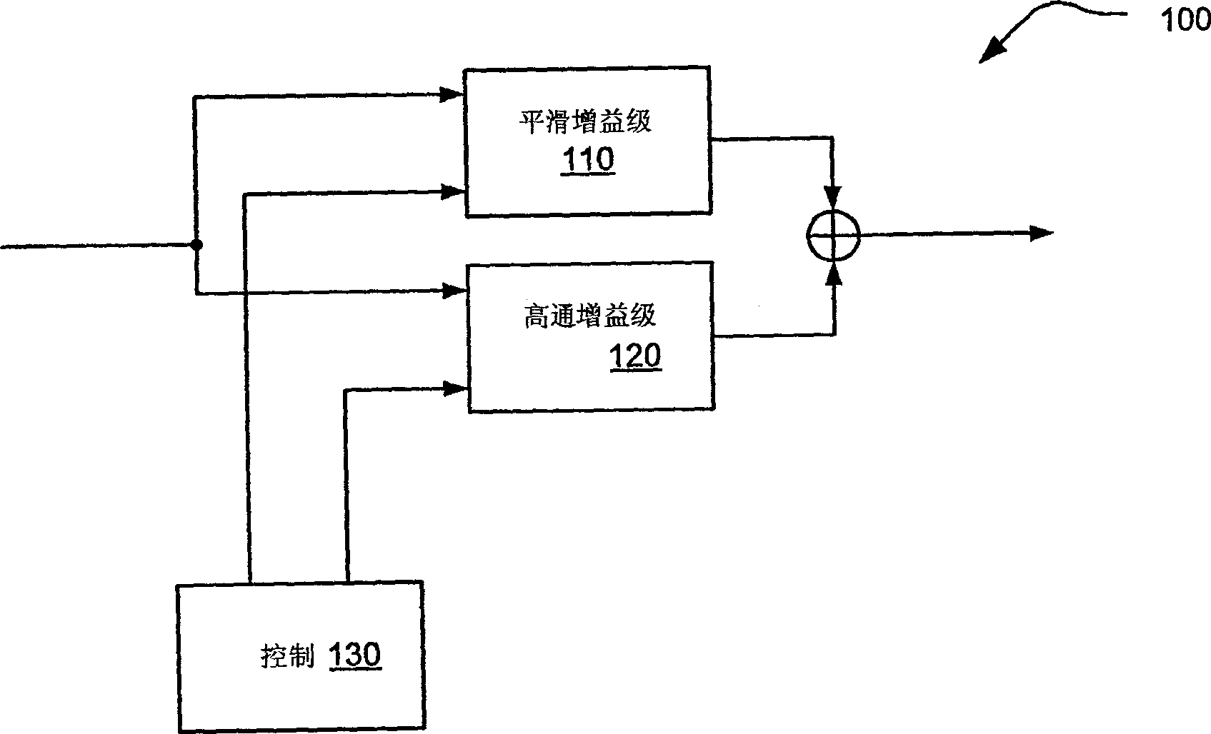
This will have the undesired and detrimental effect of reducing the bandwidth of the data path
In addition, if this merged input is directly connected to the input of the receiver, due to the additional capacitive load, the impedance matching between the input of the receiver and the PCB (printed circuit board) bonding wire will be severely reduced (that is, the lead to severe impedance mismatch)
This can lead to more undesirable and harmful effects due to the large number of reflections that can greatly reduce the integrity of the input data
Another potential problem with this prior art two-path embodiment 100 is that when signals passing through two different paths are combined in a summer, additional delays can be generated if the two paths have significantly different delays. the jitter
It can be seen that while the prior art two-path embodiment 100 at least provides a solution with adjustable gain and equalizer stages, it has significant limitations
Rather, among all other problems, the prior art two-path embodiment 100 is power-hungry, introduces undesired impedance mismatches, and great care needs to be taken to ensure that the two paths have sufficiently close time delays

Method used


Image

  • Current-controlled cmos wideband amplifier/equalizer circuit
  • Current-controlled cmos wideband amplifier/equalizer circuit
  • Current-controlled cmos wideband amplifier/equalizer circuit

Examples


Embodiment Construction

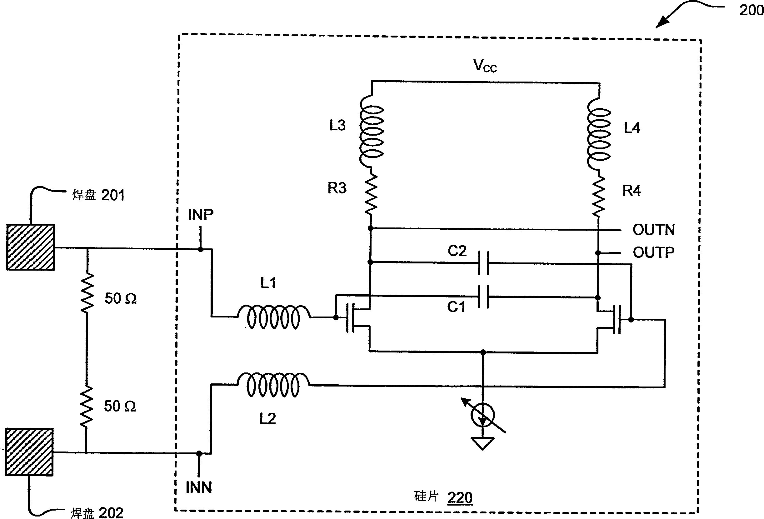
[0084] Embodiments of the present invention relate to ultra high speed logic circuits applied to silicon complementary metal oxide semiconductor (CMOS) processing technology. A distinction is made here between the terms "CMOS process technology" and "CMOS logic". The CMOS processing technology used here generally refers to various mature CMOS manufacturing processes, which construct field effect transistors on silicon substrates with gate leads, which are usually made of polysilicon material placed on insulating material As made on silica. CMOS logic, on the other hand, refers to the use of complementary CMOS transistors (N-channel and P-channel) to form various logic gates and more complex logic circuits in which zero quiescent current is consumed. Various embodiments of the present invention use the current control mechanism to develop a series of very fast current control CMOS (C3MOS or CMOS 3 MOS TM ) logic, which can be fabricated with various conventional CMOS process...


PUM


Abstract

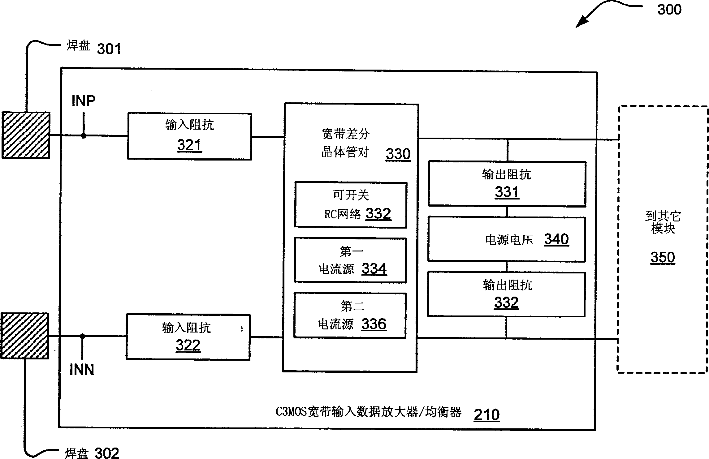
Current-controlled CMOS (C3MOS) fully differential integrated wideband amplifier / equalizer with adjustable gain and frequency response without additional power or loading. A novel approach is presented by which adjustable amplification and equalizer may be achieved using a C3MOS wideband data stage. This may be referred to as a C3MOS wideband data amplifier / equalizer circuit. This employs a wideband differential transistor pair that is fed using two separate transistor current sources. A switchable RC network is communicatively coupled between the sources of the individual transistors of the wideband differential transistor pair. There are a variety of means by which the switchable RC network may be implemented, including using a plurality of components (e.g., capacitors and resistors connected in parallel). In such an embodiment, each component may have an individual switch to govem its connectivity in the switchable RC network thereby allowing a broad range of amplification and equalization to be performed.

Description

technical field [0001] The present invention relates to communication devices, and more particularly to amplification and equalization techniques applied in said communication devices. Background technique [0002] The development of high-speed circuit technologies such as current-controlled CMOS (or C3MOS) logic has brought significant increases in the speed of circuits fabricated using standard CMOS processing techniques. [0003] In order to adapt the communication system to various input data communication channel types, wideband data amplifiers are required to provide high-pass responses with different amplification levels while providing a smooth frequency response. In another embodiment (US Patent Application Publication No. 20040028158), two separate paths are provided for input data: (1) one with a smooth frequency response (2) the other with a high pass frequency response. After passing through these two paths, the signals are combined at the summing stage. The r...

Claims


Application Information

Patent Timeline
Patent Type & Authority Applications(China)
IPC IPC(8): H03F1/14H03F1/48
Inventor 曹军
Owner AVAGO TECH INT SALES PTE LTD
Learn More