Method for raising radiation of silicone based crystal thin film by use of process of plasma

A plasma and thin film technology, applied in semiconductor devices, electrical components, circuits, etc., can solve the problems of breaking the parity selection rule, changing the spectral wavelength and intensity, etc., to achieve the effect of simple and easy preparation and process compatibility

Inactive Publication Date: 2007-02-21
INST OF SEMICONDUCTORS - CHINESE ACAD OF SCI
View PDF0 Cites 2 Cited by
  • Summary
  • Abstract
  • Description
  • Claims
  • Application Information

AI Technical Summary

Problems solved by technology

For free electrons Er 3+ , the electric dipole transition between 4f energy levels is forbidden, but the crystal field will make the doped Er 3+ Energy level splitting of ions, which violates the parity selection rule, thereby changing the wavelength and intensity of the spectrum

Method used


Image

  • Method for raising radiation of silicone based crystal thin film by use of process of plasma
  • Method for raising radiation of silicone based crystal thin film by use of process of plasma
  • Method for raising radiation of silicone based crystal thin film by use of process of plasma

Examples


Embodiment 1

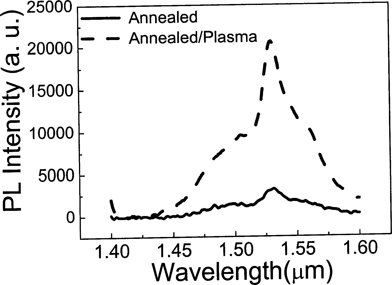
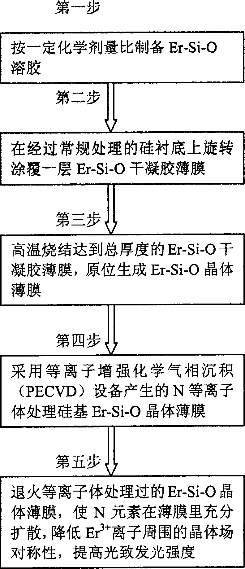
[0025] image 3 A method for improving the luminescence of silicon-based crystal thin films by plasma treatment, the steps are as follows:

[0026] The first step is to prepare Er-Si-O sol according to a certain stoichiometric ratio

[0027] The preparation process is to take 4.5ml of ethyl orthosilicate according to the chemical dosage under the constant temperature condition of 50°C, and then add the mixed solution H containing water and ethanol. 2 O / C 2 h 5 OH 27ml (where H 2 O 4.5ml, C 2 h 5 OH 22.5ml), magnetically stirred for 1 h to mix the solution evenly and hydrolyze TEOS to obtain a network structure. Weigh ErCl according to chemical dosage 3 .6H 2 O powder 11.451g (0.03mol), add 40ml of C 2 h 5 OH, with magnetic stirring for 30min, to make ErCl 3 saturated solution. ErCl 3 Add the saturated solution of TEOS, H 2 O, C 2 h 5 Mix the solution with OH and stir it magnetically for 4 h to make the solution evenly mixed.

[0028] In the second step, a laye...


PUM


Abstract

Specially, the invention is related to method for raising luminescence of silicon based crystal thin film by using process of plasma. The method includes steps: (1) preparing Er-Si-O sol according to certain ratio of chemical dose; (2) spin coating a layer of thin film of Er-Si-O dried gel xerogel on conventional processed silicon substrate; (3) high sintering to reach total thickness of thin film of Er-Si-O dried gel xerogel, and generating thin film of Er-Si-O crystal in situ; (4) processing thin film of silicon based Er-Si-O crystal by using N plasma produced by equipment of plasma enhanced chemical vapor deposition (PECVD); (5) two times of annealing thin film of Er-Si-O crystal processed by plasma in order to diffuse N element in thin film well, lower symmetry of crystal field around Er3+ ions, and raise intensity of photoluminescence.

Description

technical field [0001] The invention relates to the technical field of preparation and application of optoelectronic thin film materials and devices. In particular, a method for enhancing the luminescence of silicon-based crystal thin films by plasma treatment. Background technique [0002] With the nanometer size of silicon-based microelectronic devices and the ultra-large scale of integrated circuits, the delay of electronic circuit interconnection will become a "bottleneck" in the development of microelectronic technology, which will seriously limit the response rate of electronic devices and cannot meet the requirements of information processing, transmission and storage. bit rate (Tb / s) needs. The use of optical interconnection will help improve system response rate, cross-connection density, information processing speed and accuracy, while reducing electromagnetic wave crosstalk and energy loss. To achieve optoelectronic integration, the primary task is to find effic...

Claims


Application Information

Patent Timeline
IPC IPC(8): H01L33/00
Inventor 王晓欣张建国王启明
Owner INST OF SEMICONDUCTORS - CHINESE ACAD OF SCI
Why Eureka
Try Eureka