Organic electroluminescence display unit

An electroluminescence and organic technology, applied in the field of active organic electroluminescence displays, can solve the problems of the influence of the performance of the organic electroluminescence diode 80, the reduction of the aperture ratio of the unit pixel 70, and the hindering of the display performance of the display.

Active Publication Date: 2006-09-13
테스콤가부시키가이샤
View PDF0 Cites 9 Cited by
  • Summary
  • Abstract
  • Description
  • Claims
  • Application Information

AI Technical Summary

Problems solved by technology

[0008] Regarding the current driving characteristics of the organic electroluminescent diode 80, those skilled in the art related to this case will know that if the first transistor 73 is fabricated by an amorphous silicon (α-Si) process, due to the electron mobility of amorphous silicon (mobility) Relatively weak, for example, its electron transfer efficiency may only be one-thousandth of that of low-temperature polysilicon, so the performance of the organic light-emitting diode 80 is also affected.
If it is desired to increase the size of the first transistor 73 (especially the size of the semiconductor channel region), or to add an additional transistor (of course, this additional transistor is arranged side by side with the first transistor 73) The amount of current supplied to the organic light-emitting diode 80, because these methods will reduce the aperture ratio of the unit pixel 70, which will hinder the display performance of the display, and there are difficulties in practical implementation.

Method used


Image

  • Organic electroluminescence display unit
  • Organic electroluminescence display unit
  • Organic electroluminescence display unit

Examples


Embodiment Construction

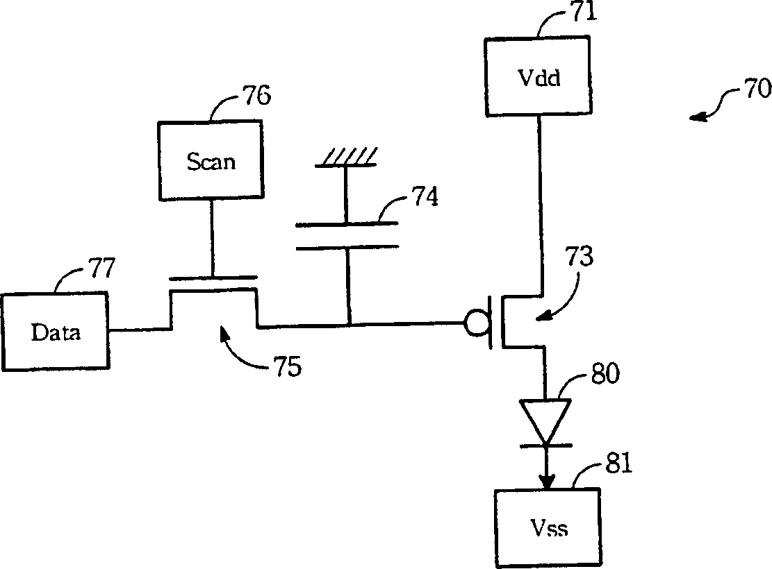
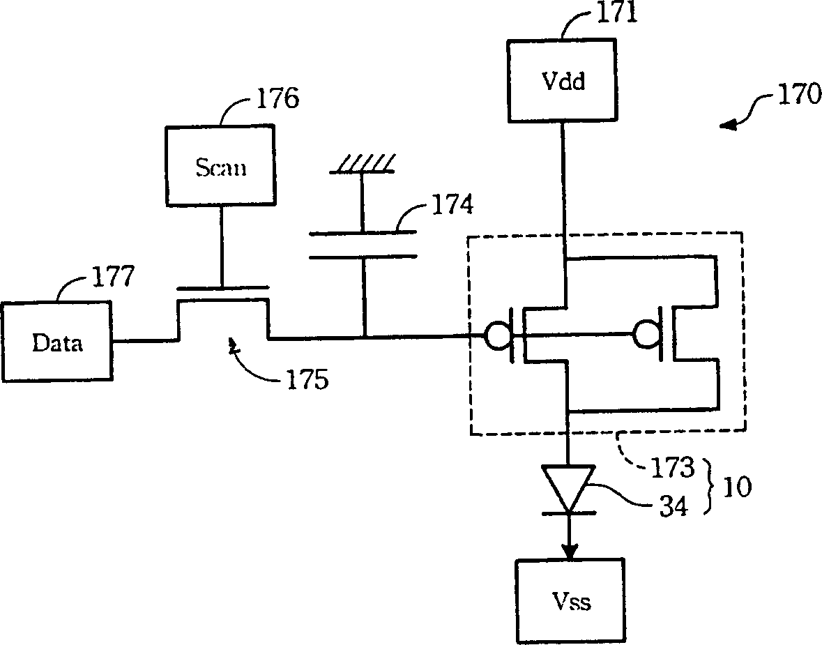
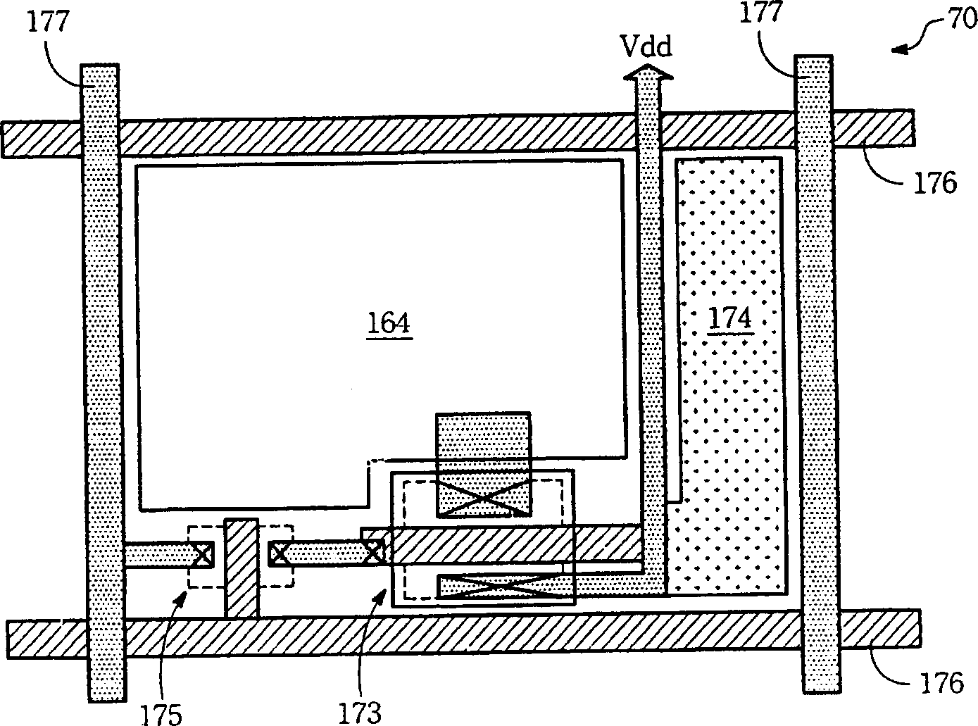
[0039] Please refer to figure 2 , which is an equivalent circuit diagram of the unit pixel 170 in the active organic electroluminescence display provided by the present invention. The unit pixel 170 includes the organic electroluminescence display unit 10 , a capacitor 174 and a second thin film transistor 175 . The organic electroluminescent display unit 10 includes an organic electroluminescent diode 34 and a first thin film transistor 173 . It is worth mentioning that the first thin film transistor 173 provided by the present invention is a thin film transistor with a double channel, which is compared with the traditional thin film transistor (of course, under the premise of other process conditions being the same) , the first thin transistor 173 of the present invention can generally provide twice the amount of current, so on the equivalent circuit diagram, this characteristic is represented by the symbol of two transistors connected in parallel.

[0040] During operati...


PUM


Abstract

This invention provides an organic electroluminescent display unit including a base plate, a first non-crystalline silicon layer, a grating metal, a second non-crystalline silicon layer, a first passive layer and an organic electroluminescent diode, in which, the first non-crystalline silicon layer is set on the base plate including a first channel region, a first source/drain region and a second source/drain region, the grating metal is set above the first channel region, the second non-crystalline silicon layer includes a second channel region, a third source/drain and a fourth source/drain region, in which, the second channel is set above the grating metal, the first passive layer covers the first non-crystalline silicon layer, the grating metal and the second non-crystalline silicon layer on the base board, the diode is set on the passive layer and connected with the first and third source/drain metals electrically.

Description

technical field [0001] The present invention relates to an organic electroluminescence display, in particular to an active organic electroluminescence display. Background technique [0002] Organic electroluminescent displays have been actively researched and discussed in display technology recently, which can be used to make thin displays, and compared to another thin display, the liquid crystal display, organic electroluminescent diodes As a self-luminous component, the liquid crystal display requires a backlight. Therefore, the organic electroluminescent display can not only further reduce the size of the liquid crystal display, but also easily achieve better optical effects, such as more saturated color reproduction. Spend. [0003] The organic electroluminescent diode is usually a multilayer film structure composed of organic materials, and its typical condition usually includes a hole injection layer, a hole transport layer, a light-emitting layer, an electron transpo...

Claims


Application Information

Patent Timeline
Patent Type & Authority Applications(China)
IPC IPC(8): H01L27/32
Inventor 姚智文
Owner 테스콤가부시키가이샤
Why Eureka
Try Eureka