Method for solving CSLICLBOL integrated circuit fail by PMOS pipe

A technology of integrated circuits and circuits, applied in the manufacture of circuits, electrical components, semiconductors/solid-state devices, etc.

Inactive Publication Date: 2004-07-07
SHANGHAI BEILING
View PDF0 Cites 2 Cited by
  • Summary
  • Abstract
  • Description
  • Claims
  • Application Information

AI Technical Summary

Problems solved by technology

[0005] The technical problem to be solved by the present invention is to provide a PMOS transistor to solve the failure method of the CSLIC1B01 integrated circuit, so as to overcome the problems existing in the prior art

Method used


Image

  • Method for solving CSLICLBOL integrated circuit fail by PMOS pipe
  • Method for solving CSLICLBOL integrated circuit fail by PMOS pipe
  • Method for solving CSLICLBOL integrated circuit fail by PMOS pipe

Examples


Embodiment Construction

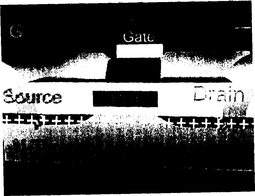
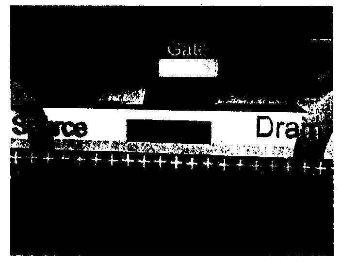
[0010] Such as figure 1 As shown, when a negative voltage is applied to the gate (Gate), many holes will be induced in the thin area under the oxide layer and gradually gather together; when a bias voltage is applied to the source (Source), The accumulated holes conduct (channel) through the channel between the source (Source) and the drain (Drain), generating a current. The magnitude of the PMOS tube current is inversely proportional to its channel length (L), that is, the longer the channel length, the smaller the current. On the contrary, the shorter the channel length, the greater the current. By changing the length of the channel, the PMOS tube can be changed. The size of the conduction current.

[0011] The present invention changes the channel length of the PMOS transistor (MPD5) from 10 μm to 8 μm, thereby increasing its current flow, so that it has sufficient ability to drive the next stage circuit.

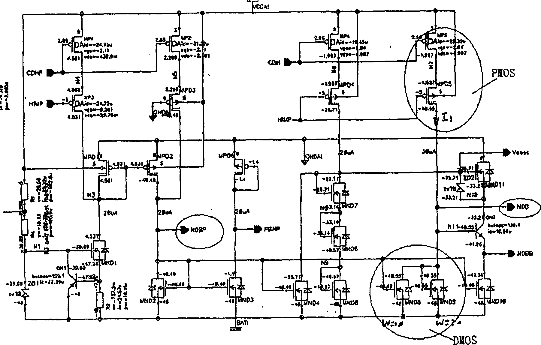
[0012] figure 2 It is CSLIC1B01 integrated circuit, including D...


PUM


Abstract

The present invention discloses a method for solving the failure of CSLIC1B01 integrated circuit with respect to PMOS transistor. DMOS integrated circuit is one of the high voltage integrated circuit in the field of micro-electronic circuit used widely in the communication. The invention increases the general current I1 by a big margin by changing the dimension of the PNOS transistor on the key path of the CSLIC1B01 integrated circuit and adjusting the current passing through the path, so that NDB has the enough ability to drive the circuit of next stage, eliminating the failure of the integrated circuit due to mismatch of the DMOS circuit.

Description

technical field [0001] The invention relates to a CSLIC1B01 integrated circuit. Background technique [0002] DMOS tube circuit is one of the high-voltage integrated circuit tubes, which belongs to a kind of microelectronic circuit, which is widely used in the field of communication. [0003] DMOS tubes can have very short channels, and can not rely on photolithography mask process technology to determine the channel length. This structure enables punchthrough to be well controlled due to the heavily doped shielding region. The lightly doped drift region achieves speed saturation by maintaining a uniform electric field, so that the voltage drop in this region is minimized. The electric field near the drain region is the same as the electric field in the drift region, so compared with conventional MOSFETs and HMOSs, its avalanche breakdown, multiplication and oxide charging are all weakened. Therefore, its main features are high threshold and high withstand voltage, and it...

Claims


Application Information

Patent Timeline
IPC IPC(8): H01L21/82H01L29/78
Inventor 谈毅平聂纪平朱朝晖谢玉森戚盛勇蔡敏
Owner SHANGHAI BEILING
Why Eureka
Try Eureka