
Improved DDR II dram data path

A technology for storage devices and memory arrays, which is applied in the access field of storage devices and can solve problems such as reduced speed performance, gate delay, large mask area, etc.

Inactive Publication Date: 2006-08-30
INFINEON TECH AG +1
View PDF0 Cites 7 Cited by
  • Summary
  • Abstract
  • Description
  • Claims
  • Application Information

AI Technical Summary

Problems solved by technology

Unfortunately, synthetic designs have disadvantages
For example, it typically puts all combinatorial logic together, which incurs larger gate delays and larger mask areas, which impacts performance and density
Also, timing disturbances and unnecessary switching operations in these designs often degrade speed performance and increase power consumption
These timing issues get worse as the clock frequency increases
Furthermore, the typically unsystematic nature of synthetic design logic does not facilitate reuse, for example, across device family members with different architectures (e.g., ×4, ×8, and ×16) or within individual devices supporting different architectures

Method used


Image

  • Improved DDR II dram data path
  • Improved DDR II dram data path
  • Improved DDR II dram data path

Examples


Embodiment Construction

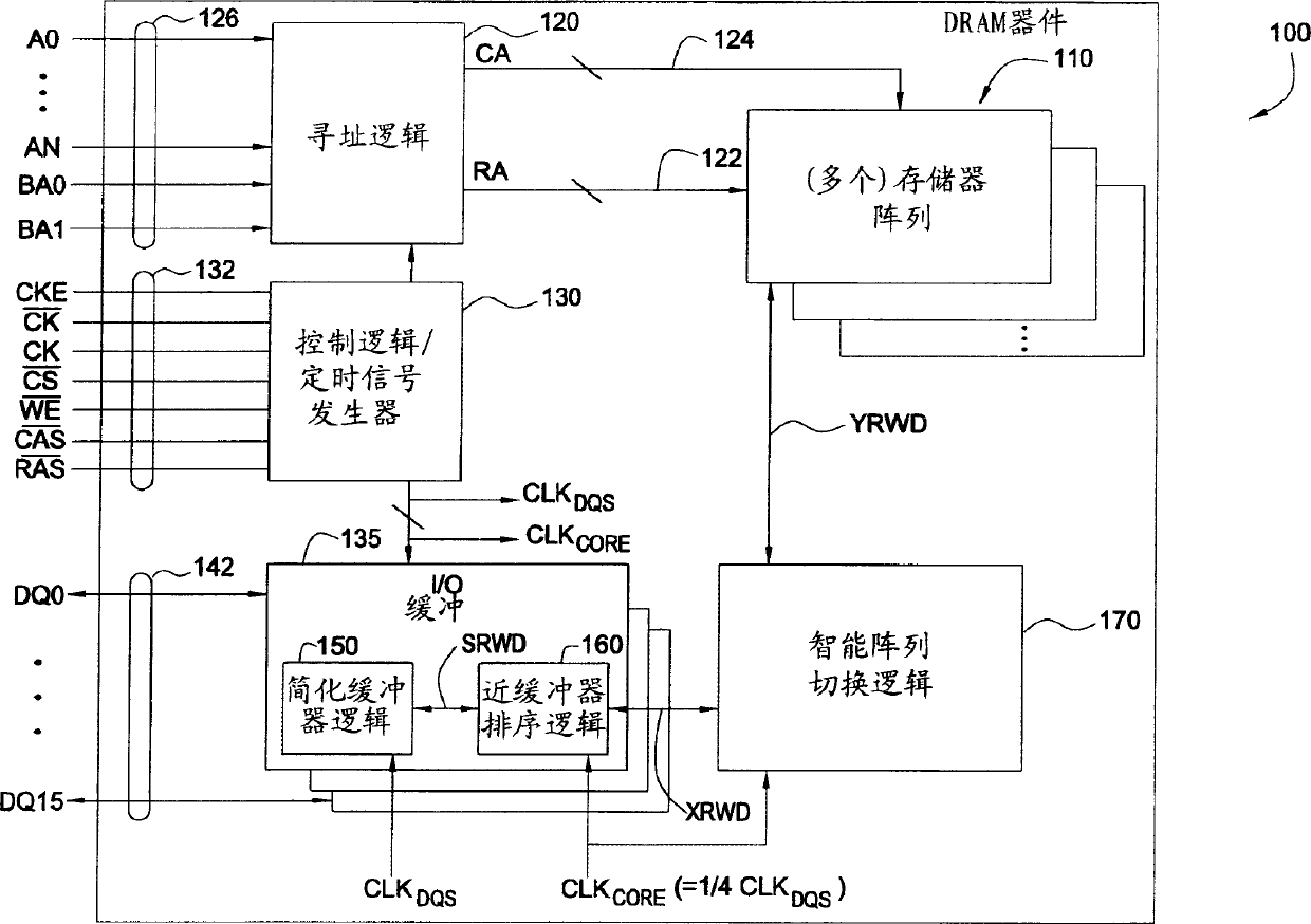
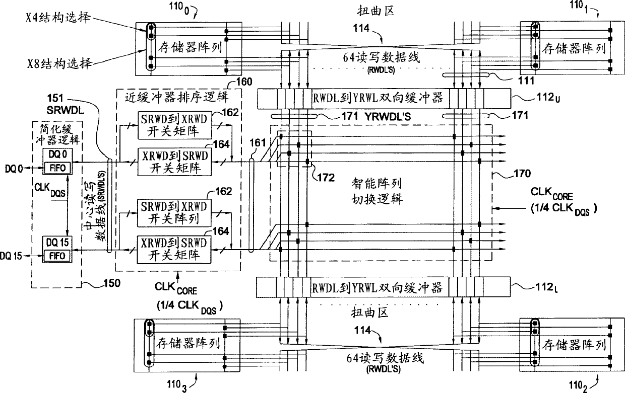
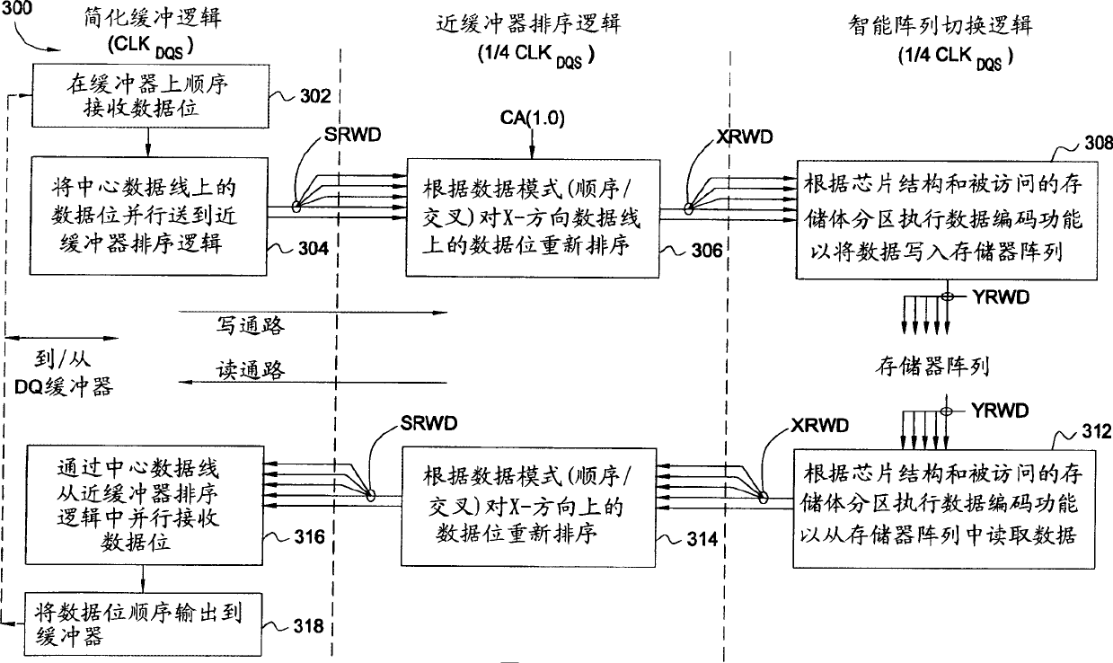
[0029] Embodiments of the present invention primarily provide techniques and circuits to support the switching operations required to transfer data between a memory array / bank and an external data buffer. On the write path, these switching operations include latching and assembling multiple bits received consecutively through a single data buffer, pairing them based on a particular type of access (e.g., interleaved or sequential, odd / even). The bits are reordered and coded based on the bank location accessed by the chip structure (eg ×4, ×8 or ×16). On the read path, similar operations can be performed (in reverse order) to prepare and assemble the data to be read from the device.

[0030] In the data path, by distributing these switching operations between different logic blocks, only some operations (such as latching data) can be performed at the data clock frequency, while the remaining operations (such as sorting and encoding) are performed at lower frequencies (such as 1...


PUM


Abstract

An improved doubled data rate (DDR)-II type dynamic random access memory (DRAM) device data path is disclosed. Techniques and circuitry that support switching operations required to exchange data between memory arrays and external data pads are provided. In a write path, such switching operations may include latching in and assembling a number of bits sequentially received over a single data pad, reordering those bits based on a type of access mode (e.g., interleaved or sequential), and performing scrambling operations based on chip organization (e.g., x4, x8, or x16) a bank location being accessed. Through separation the high speed buffer logic from switching logic which can perform other various logic functions, the switching logic performing the functions can work under a lower clock frequency, thus the time that data is transmitted from the memory arrays to the DQ pads is saved and associated timing requirements is relaxed and the latency is improved, otherwise.

Description

technical field [0001] The present invention relates generally to accessing memory devices, and more particularly, to accessing double data rate (DDR) dynamic random access memory (DRAM) devices, such as DDR-II type DRAM devices. Background technique [0002] The development of submicron CMOS technology has led to an increase in demand for high speed semiconductor memory devices, such as dynamic random access memory (DRAM) devices, pseudo static random access memory (PSRAM) devices, and the like. Here, this type of memory is collectively referred to as a DRAM device. [0003] Some types of DRAM devices have a synchronous interface, which usually means that data is written to or read from the device along with clock pulses. Early synchronous DRAM (SDRAM) devices transferred one bit of data per clock cycle (eg, on the rising edge), and were properly referred to as single data rate (SDR) SDRAM devices. Later, improved double data rate (DDR) SDRAM devices included input / output...

Claims


Application Information

Patent Timeline
Patent Type & Authority Applications(China)
IPC IPC(8): G11C11/409G11C11/4093G11C11/4096
CPCG11C7/1078G11C7/1096G11C7/1087G11C7/1018G11C7/222G11C11/4076G11C11/4093G11C11/4096
Inventor K·费基-罗姆德汉S·S·刘
Owner INFINEON TECH AG
Learn More