High depth-width ratio deep sub-micrometer, nanometer metal structure making process based on self-supporting thin film

A self-supporting thin film, deep submicron technology, applied in nanostructure manufacturing, photoengraving process of pattern surface, nanotechnology, etc. It is difficult to achieve and other problems to achieve the effect of strong practical value

Active Publication Date: 2006-07-12
SEMICON MFG INT (SHANGHAI) CORP +1
View PDF0 Cites 11 Cited by
  • Summary
  • Abstract
  • Description
  • Claims
  • Application Information

AI Technical Summary

Problems solved by technology

[0002] For phase diffractive optical elements in the high-precision X-ray band, in order to obtain the required phase, it is necessary to fabricate high-aspect ratio deep submicron and nanometer metal structures. As we all know, due to the limitation of resolution and electron energy, conventional electron beam light The engraving process canno...

Method used


Image

  • High depth-width ratio deep sub-micrometer, nanometer metal structure making process based on self-supporting thin film
  • High depth-width ratio deep sub-micrometer, nanometer metal structure making process based on self-supporting thin film
  • High depth-width ratio deep sub-micrometer, nanometer metal structure making process based on self-supporting thin film

Examples


Embodiment

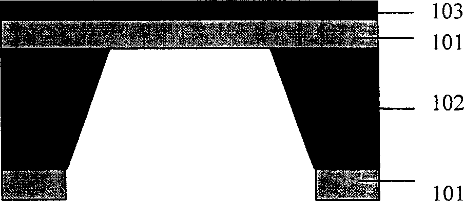
[0033] 1. If diagram 2-1 As shown, firstly, a thin chromium and thin gold layer 203 is deposited on the front surface of the п-shaped self-supporting film. The thin chromium and thin gold layer 203 can be obtained by electron beam evaporation, with a total thickness of 10-30 nm. The п-shaped self-supporting film is composed of a silicon nitride film 101 and a silicon wafer 102, the bottom leg is a silicon nitride film 101, the middle leg is a silicon wafer 102, and the upper end is a silicon nitride film 101.

[0034] 2. If Figure 2-2 As shown, the electron beam glue 204 is thrown on the surface of the thin chrome and thin gold layer 203. The model of the electron beam glue 204 is SAL601-ER7 produced by Japan Shipley Company. , the pre-baking temperature is 105°C, and the pre-baking time is 2 minutes.

[0035] 3. Figure 2-3 As shown, the electron beam glue 204 is subjected to electron beam exposure, the dose is 35 microcoulombs, and then the electron beam glue 204 is pos...


PUM

PropertyMeasurementUnit
Thicknessaaaaaaaaaa
Thicknessaaaaaaaaaa
Thicknessaaaaaaaaaa

Abstract

The invention bases on metal structure manufacture technology of deep sub-micron and nanometer for high aspect ratio of self-support film comprises: 1. depositing thin Cr and Au on front face of self-support film; 2. whirling electron micelle on thin Cr/Au surface to exposure and develop the electron beam; 3. putting the slice into electroplate liquid to electroplate metal firstly; 4. whirling X-ray resist on front face of slice; 5. taking X-ray exposure and develop from the film back surface; 6. electroplating secondly; 7. removing glue and Cr/Au, and completing the manufacture. This invention has strong applied value and fit to large-scale production.

Description

technical field [0001] The invention belongs to the microfabrication field in the semiconductor technology, in particular to a high aspect ratio deep submicron and nanometer metal structure manufacturing process based on a self-supporting film. Background technique [0002] For phase diffractive optical elements in the high-precision X-ray band, in order to obtain the required phase, it is necessary to fabricate high-aspect ratio deep submicron and nanometer metal structures. As we all know, due to the limitation of resolution and electron energy, conventional electron beam light The engraving process cannot produce high aspect ratio deep sub-micron and nanometer metal structures. If two electron beam lithography processes are used, not only the cost is high and the process is complicated, but also it poses a high challenge to the overlay alignment ability of the electron beam lithography machine. requirements, which are difficult to achieve in practice. Contents of the in...

Claims


Application Information

Patent Timeline
IPC IPC(8): H01L21/027H01L21/00H01L21/3205G03F7/00B82B3/00
Inventor 谢常青叶甜春陈大鹏
Owner SEMICON MFG INT (SHANGHAI) CORP
Why Eureka
Try Eureka