Method for manufacturing optical fiber array connector

A manufacturing method and connector technology, applied in the field of optical communication, can solve the problems of cumbersome procedures, connector expansion, low production efficiency, etc., and achieve the effect of simple process

Inactive Publication Date: 2006-06-21
SHANGHAI INST OF OPTICS & FINE MECHANICS CHINESE ACAD OF SCI
View PDF0 Cites 2 Cited by
  • Summary
  • Abstract
  • Description
  • Claims
  • Application Information

AI Technical Summary

Problems solved by technology

But the process is cumbersome and the production efficiency is low
In addition, with ZrO 2 For ceramics, the accuracy of the distance between the holes is ±2μm. Due to the stress during processing, the crystal structure changes from tetragonal to monoclinic during sintering, which causes the connector to expand and affects the dimensional accuracy.
The optical fiber connectors and optical fiber array connectors prepared by these methods can be reinforced with adhesives after the optical fibers are inserted, and have a relatively simple operation, but the accuracy of the distance between the holes with more than two through holes and the array of through holes is affected. Influenced by various factors in metal mold manufacturing, forming, sintering and processing, it is very difficult to control the precision below 1 μm

Method used


Image

  • Method for manufacturing optical fiber array connector
  • Method for manufacturing optical fiber array connector

Examples


Embodiment 1

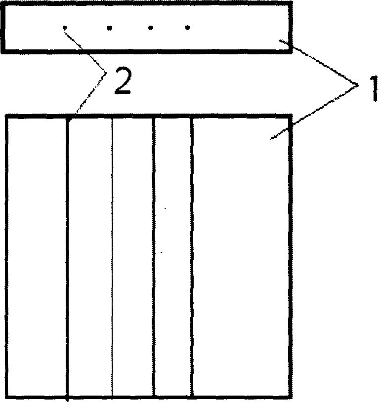
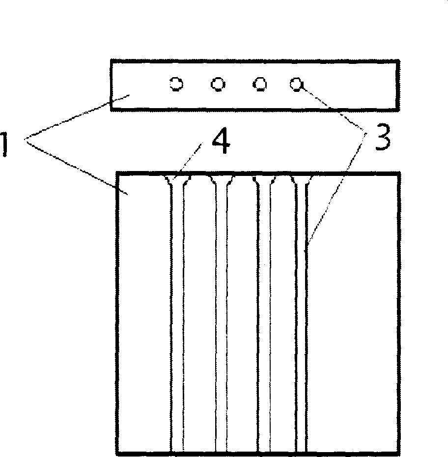
[0033] Focus a 5mW femtosecond laser with a pulse frequency of 10Hz and a wavelength of 800nm ​​on the bottom of a 5mm thick polished quartz glass with a 100x lens, and then scan from bottom to top at a speed of 5μm / s to form 2 laser beams with an interval of 250μm. × 2 wires. Then soak in 4wt% hydrofluoric acid solution, and apply ultrasonic waves, forming a through-hole array with a diameter of 125 μm and a trumpet structure on the surface. And the accuracy of the distance between the through holes is 250±1 μm. Insert the optical fiber into the hole and fix it with an adhesive to form an optical fiber array connector for optical communication.

Embodiment 2

[0035] Focus the 100mW femtosecond laser with pulse frequency of 1KHz and wavelength of 750nm on the bottom of the 5mm thick polished quartz glass with a 50 times lens, and then scan from bottom to top at a speed of 1000μm / s to form 6 laser beams with an interval of 250μm. ×6 wires. Then soak in 4wt% hydrofluoric acid solution, and apply ultrasonic waves, forming a through-hole array with a diameter of 125 μm and a trumpet structure on the surface. And the accuracy of the distance between the through holes is 250±1 μm. Insert the optical fiber into the hole and fix it with an adhesive to form an optical fiber array connector for optical communication.

Embodiment 3

[0037] Focus the 500mW femtosecond laser with pulse frequency of 200KHz and wavelength of 850nm on the bottom of 5mm thick polished quartz glass with a 2x lens, and then scan from bottom to top at a speed of 5000μm / s to form 10 laser beams with an interval of 250μm. ×10 wires. Then soak in 4wt% hydrofluoric acid solution, and apply ultrasonic waves, forming a through-hole array with a diameter of 125 μm and a trumpet structure on the surface. And the accuracy of the distance between the through holes is 250±1 μm. Insert the optical fiber into the hole and fix it with an adhesive to form an optical fiber array connector for optical communication.


PUM


Abstract

The invention discloses a fiber-optical array connector making method of optical communication, which comprises the following steps: combining the femtosecond laser illuminating and chemical disposal method to produce the array through-hole in the base plate; plugging and fixing the optical fiber in the through-hole to prepare the fiber-optical array connector. The method prevents the traditional method from preparing mould and sintering the blank, which simplifies the manufacturing technology and improves the gap precision.

Description

technical field [0001] The invention relates to optical communication, in particular to a method for manufacturing an optical fiber array connector for optical communication combined with femtosecond pulsed laser irradiation and chemical treatment. Background technique [0002] So far, the connectors and fiber array connectors used to fix optical fibers, connect optical fibers and optical communication components, and optical fibers are generally machined into V-shaped grooves on the surface of microcrystalline glass, silicon substrate, quartz glass, etc., or use ZrO 2 Ceramics are produced by using a metal mold as a blank, then sintered and finally machined to form the pores. The machining accuracy of the V-shaped groove is ±5μm. To ensure the accuracy of the V-shaped groove, it needs to be corrected by cutting and polishing. But the procedure is loaded down with trivial details, and production efficiency is low. In addition, with ZrO 2 For ceramics, the accuracy of the ...

Claims


Application Information

Patent Timeline
IPC IPC(8): G02B6/255B23K26/36G02B6/24
Inventor 姜雄伟邱建荣朱从善
Owner SHANGHAI INST OF OPTICS & FINE MECHANICS CHINESE ACAD OF SCI
Why Eureka
Try Eureka