Headlamp
A technology for headlamps and nitride semiconductors, which is applied in the direction of headlamps, lighting and heating equipment, fixed lighting devices, etc., can solve the problems of limited output, decreased light emission output, inability to stimulate multiple quantum well light emission, etc., and achieves the production cost. reduced effect
- Summary
- Abstract
- Description
- Claims
- Application Information
AI Technical Summary
Problems solved by technology
Method used
Image

Examples
no. 1 approach
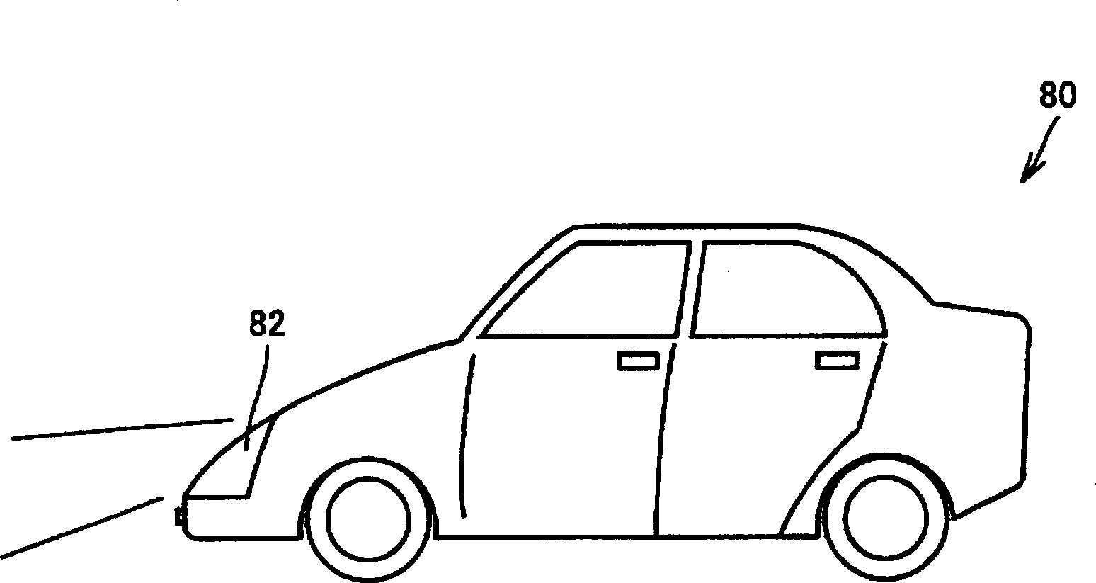
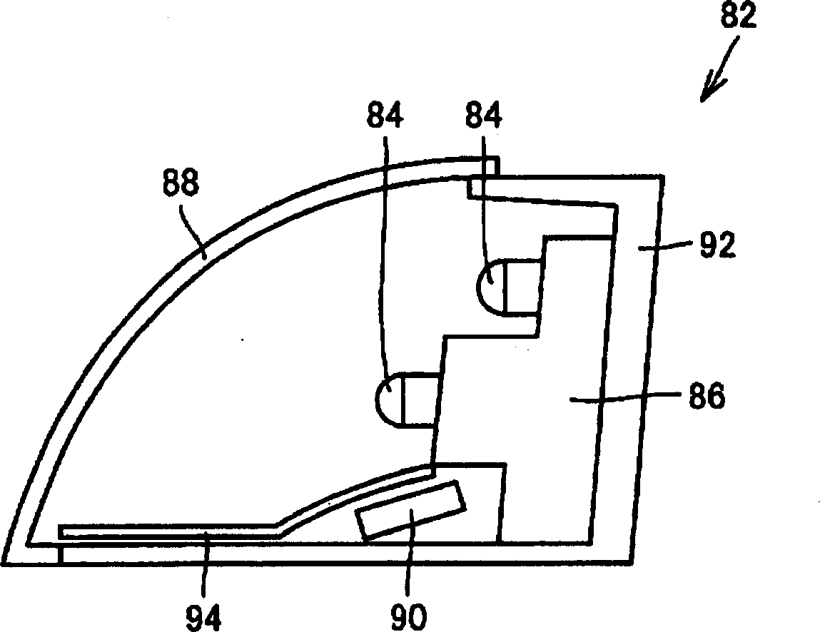
[0086] figure 1 It is a simplified schematic diagram showing a vehicle equipped with the vehicle headlight of the present invention. figure 2 is installed in the figure 1 Simplified cutaway schematic of a headlight on the vehicle shown. The following will refer to figure 1 and 2 The headlamp of the present invention is described.
[0087] Such as figure 1 As shown, a headlight 82 as a first embodiment of the present invention is disposed at the front of a vehicle body of a vehicle 80 . When the vehicle 80 is running at night or in a tunnel, the headlights 82 emit light to illuminate the front of the vehicle 80 .
[0088] Such as figure 2 As shown, the headlight 82 is equipped with two LEDs 84 which are arranged on top of the base 86 , the headlight 82 is also equipped with a rear cover 92 and a light glass 88 which form a housing for holding the base 86 . Inside the casing formed by the rear cover 92 and the lamp glass 88 are an inner reflector 94 placed under the ...
no. 1 example
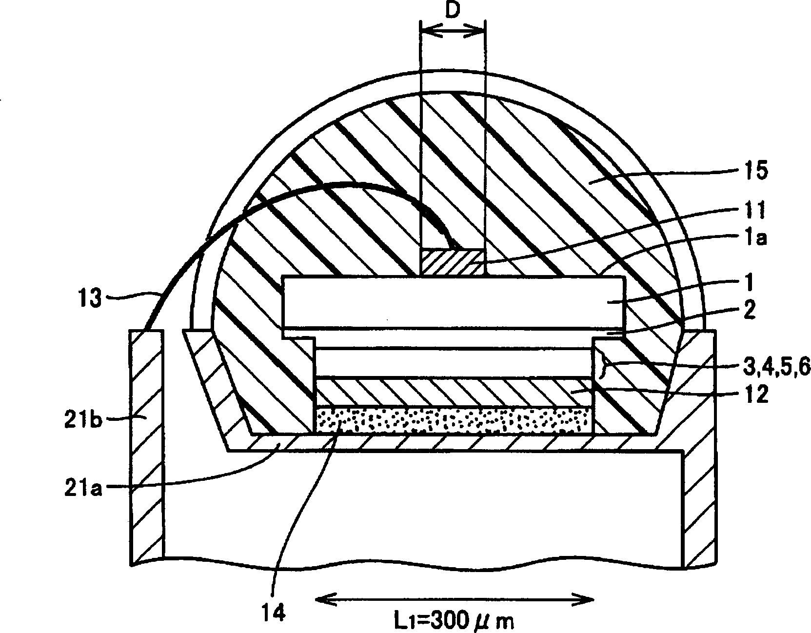
[0091] First, the LED according to the above-mentioned present invention was mounted on the headlight 82 as a light emitting device, and the GaN substrate was a nitride semiconductor substrate used in the LED 84, and this GaN substrate was compared with a sapphire substrate. image 3 The above shows a schematic diagram of the LED of the inventive sample A used in the headlight of the first embodiment of the present invention. On the first main surface of GaN substrate 1 are formed a P-electrode 12 and a layered structure including a light emitting layer, which will be described later, and the like. In this embodiment, the P-electrode 12 is mounted downwardly on the lead frame mounting part 21a by using the conductive adhesive 14 .
[0092] Second main surface 1a of GaN substrate 1 is a surface that emits light from the light emitting layer, and n-electrode 11 is provided on this surface. The n-electrode 11 does not cover the entire second main surface. It is important that m...
no. 2 example
[0125] In the second embodiment of the present invention, an inventive sample C having an enlarged area will be described. The structure of this inventive sample C is the same as image 3 Inventive Sample A shown has the same structure. However, the linear dimension L1 in Invention Sample A is 0.3 mm (300 micrometers), while in Invention Sample C it is 10 times larger to 3 mm, so its area is increased by 100 times, as Figure 13 shown. First, the method of producing Invention Sample C is as follows.
[0126] (Invention Sample C)
[0127] (c1)-(c5) Execute exactly the same corresponding steps as Inventive Sample A, but with a large GaN substrate.
[0128] (c6) On the second main surface on the GaN substrate surface side, n-electrodes having a diameter of 100 microns were formed at intervals of 3.1 mm by photolithography, evaporation and lift-off. As an n-electrode, a layered structure (20nm Ti layer / 100nm Al layer / 20nm Ti layer / 200nm Au layer) was formed in contact with th...
PUM
 Abstract
Description
Claims
Application Information
 - Generate Ideas
- Intellectual Property
- Life Sciences
- Materials
- Tech Scout
- Unparalleled Data Quality
- Higher Quality Content
- 60% Fewer Hallucinations
Browse by: Latest US Patents, China's latest patents, Technical Efficacy Thesaurus, Application Domain, Technology Topic, Popular Technical Reports.
© 2025 PatSnap. All rights reserved.Legal|Privacy policy|Modern Slavery Act Transparency Statement|Sitemap|About US| Contact US: help@patsnap.com