Method of manufacturing light-emitting device, and evaporation donor substrate
a technology of light-emitting devices and donor substrates, which is applied in the direction of diffusion transfer processes, instruments, photosensitive materials, etc., can solve the problems of increasing the region of the transfer layer, which is to be transferred, and achieves the improvement of definition, high precision, and the effect of increasing the number of pixels
- Summary
- Abstract
- Description
- Claims
- Application Information
AI Technical Summary
Benefits of technology
Problems solved by technology
Method used
Image
Examples
embodiment mode 1
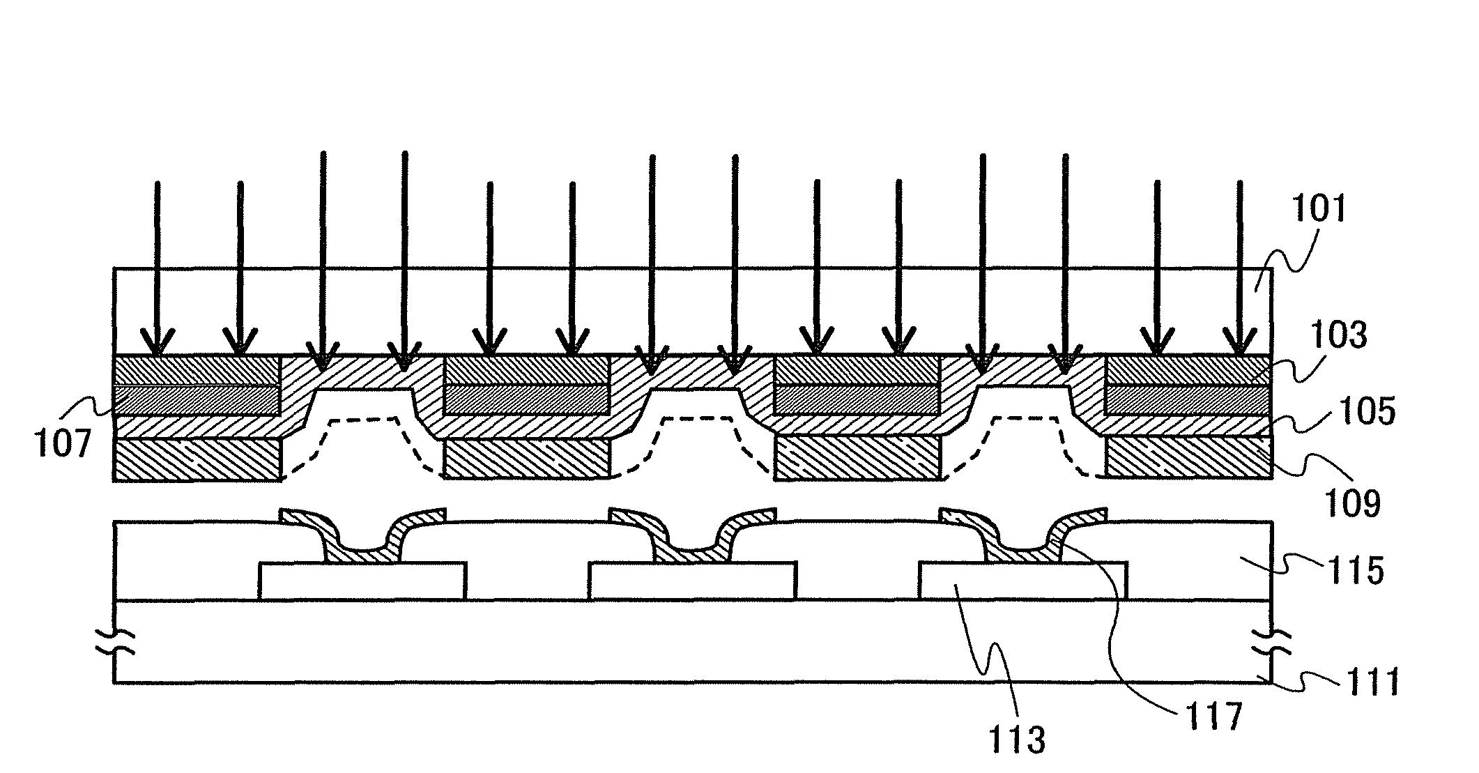
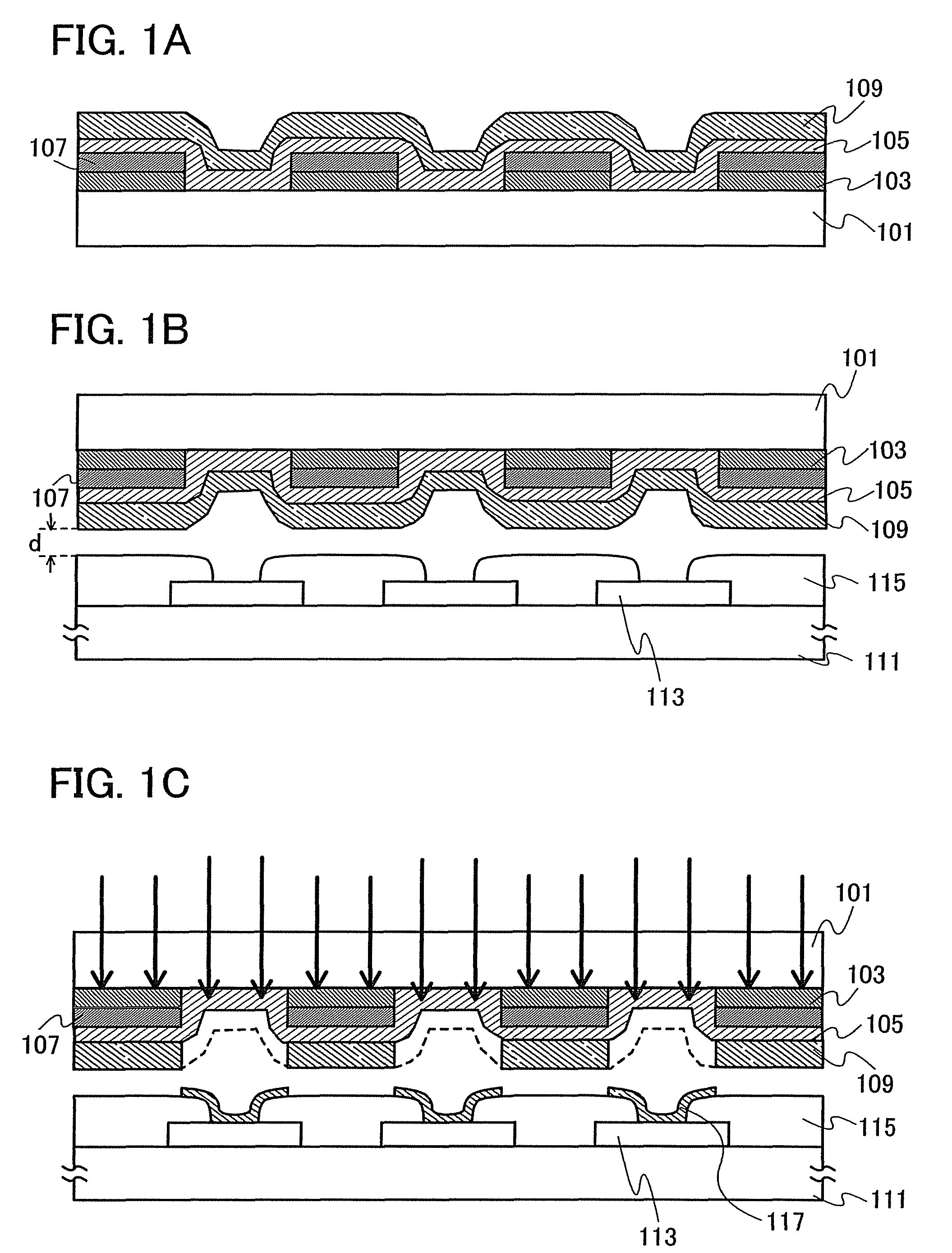
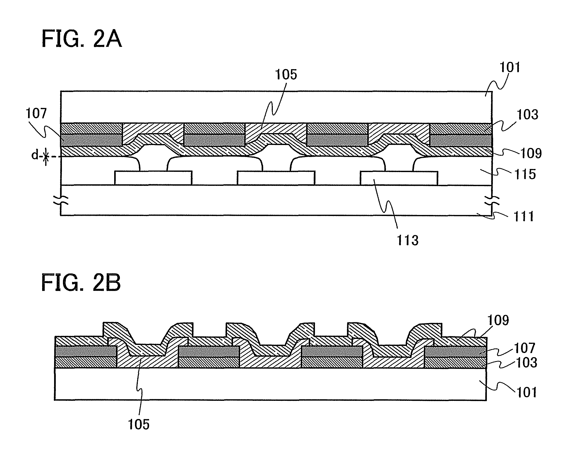
[0045]An evaporation donor substrate and a manufacturing method of a light-emitting device of the present invention are described using FIGS. 1A to 1C.
[0046]FIG. 1A shows one example of an evaporation donor substrate of the present invention. In FIG. 1A, a reflective layer 103 is formed over a first substrate 101 which is a supporting substrate. The reflective layer 103 includes an opening portion. In addition, a heat insulating layer 107 is formed over the reflective layer 103 and includes an opening portion in a region overlapped with the opening portion included in the reflective layer 103. In addition, a light absorption layer 105 is formed over the heat insulating layer 107. In FIGS. 1A to 1C, the light absorption layer 105 is formed so as to cover the entire surface of the first substrate 101. In addition, over the light absorption layer 105, a material layer 109 containing an evaporation material is formed.
[0047]Note that in this specification, “overlapped with” means not onl...
embodiment mode 2
[0092]In this embodiment mode, an evaporation donor substrate of the present invention, which differs in structure from the evaporation donor substrate in the above embodiment mode, is described. Note that when there is no particular description, the evaporation donor substrate described in this embodiment mode is formed using a material and a manufacturing method similar to the material and the method in the above embodiment mode.
[0093]FIG. 3A shows one example of an evaporation donor substrate of the present invention. In FIG. 3A, the reflective layer 103 including an opening portion is formed over the first substrate 101 which is the supporting substrate. In addition, the light absorption layer 105 is formed over the entire surface of the first substrate 101 so as to cover the opening portion in the reflective layer 103. The heat insulating layer 107 is formed over the light absorption layer 105 and includes an opening portion in a region overlapped with the opening portion inclu...
embodiment mode 3
[0106]In this embodiment mode, a manufacturing method of a full-color display device by using any evaporation donor substrate used in the above embodiment modes is described.
[0107]Although an example in which deposition is performed onto adjacent the first electrode layers 113 in a single deposition process is described in each of Embodiment Modes 1 and 2, when a full-color display device is manufactured, light-emitting layers for emitting light of different colors are formed in different regions through a plurality of deposition steps.
[0108]A manufacturing example of a light-emitting device capable of full color display is described below. Here, an example of a light-emitting device using light-emitting layers for emitting light of three colors is described.
[0109]Three evaporation donor substrates shown in FIG. 1A, FIG. 2B, FIG. 3A, or FIG. 3C are prepared. In the evaporation donor substrates, layers containing different kinds of evaporation materials are formed. Specifically, a fi...
PUM
| Property | Measurement | Unit |
|---|---|---|
| thickness | aaaaa | aaaaa |
| thickness | aaaaa | aaaaa |
| reflectance | aaaaa | aaaaa |
Abstract
Description
Claims
Application Information
 - R&D
- Intellectual Property
- Life Sciences
- Materials
- Tech Scout
- Unparalleled Data Quality
- Higher Quality Content
- 60% Fewer Hallucinations
Browse by: Latest US Patents, China's latest patents, Technical Efficacy Thesaurus, Application Domain, Technology Topic, Popular Technical Reports.
© 2025 PatSnap. All rights reserved.Legal|Privacy policy|Modern Slavery Act Transparency Statement|Sitemap|About US| Contact US: help@patsnap.com


