
Memory chip internal power administrative framework in deep shutdown mode

A memory and deep technology, applied in the direction of information storage, static memory, digital memory information, etc., can solve the problem that the low current goal is difficult to achieve and other problems

Inactive Publication Date: 2006-05-31
ETRON TECH INC
View PDF2 Cites 2 Cited by
  • Summary
  • Abstract
  • Description
  • Claims
  • Application Information

AI Technical Summary

Problems solved by technology

This low current target is not easy to achieve and requires an internal power management architecture

Method used


Image

  • Memory chip internal power administrative framework in deep shutdown mode
  • Memory chip internal power administrative framework in deep shutdown mode
  • Memory chip internal power administrative framework in deep shutdown mode

Examples


Embodiment Construction

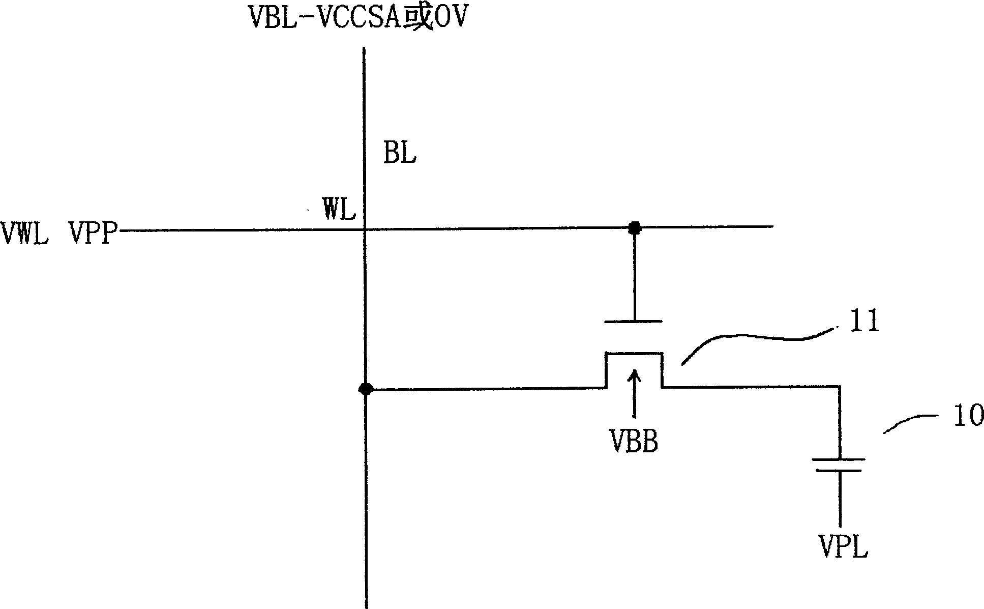
[0026] Figure 1A Shown in is the circuit diagram of the DRAM memory cell with the voltage used in the enabled state of the present invention. The bit line voltage VBL is connected to the sense amplifier voltage, which depends on the bit line data and is equal to VCCSA or 0 volts. The word line voltage VWL of the memory cell in the enabled state is VPP, and the panel voltage VPL coupled to the storage capacitor 10 is a voltage lower than the bit line sense amplifier power supply voltage VCCSA, and is generally a bit line sense Half the value of the amplifier voltage VCCSA. The base voltage VBB of the enabling unit 11 is lower than 0 volts.

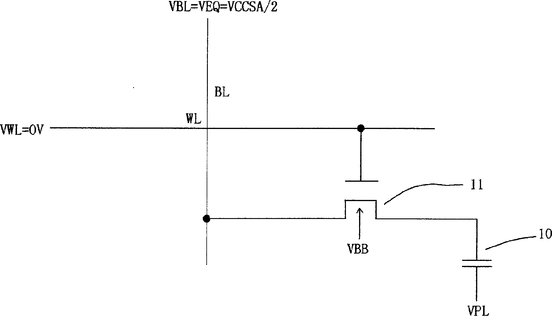
[0027] Figure 1B Shown in is the circuit diagram of the DRAM memory cell with the voltage used in the precharge state of the present invention. The bit line voltage VBL is coupled to the voltage VEQ (the equal voltage of the bit line sense amplifier), which is lower than the bit line sense amplifier power supply voltage VCCSA, and is genera...


PUM


Abstract

A depth turn ¿C off method of memory wafer includes switching off voltage regulator and charge pumping circuit, making suspension joint on memory unit voltage and using voltage obtained by external water voltage to replace internal power supply voltage of supporting circuit i.e. entering all memory units to precharge state before depth turn ¿C off mode is entered and making memory unit be suspension ¿C joint after depth turn ¿C off mode is entered to use depth turn ¿C off signal to control circuit of connecting voltage obtained by external wafer to supporting circuit.

Description

Technical field [0001] The present invention relates to a memory chip, and particularly relates to a memory chip in a deep shutdown mode. Background technique [0002] The application of low-power computing components (including memory) has continued to increase. As the performance and size of memory components increase, the power consumed by these components will increase. This will increase the burden on batteries that need to provide power for memory and other computing components. With the increase in power and performance, and the need to generate more energy, a new demand for deep shutdown modes has been generated. When in deep shutdown mode, the chip can only be allowed to consume a very small amount of standby power, which requires the chip current to be less than about 3μA. This low current goal is not easy to achieve and requires an internal power management architecture. The deep shutdown of the memory element is different from the shutdown. When the memory element is ...

Claims


Application Information

Patent Timeline
Patent Type & Authority Applications(China)
IPC IPC(8): G11C11/401G11C7/00G11C11/41
Inventor 丁达刚王明弘许人寿戎博斗
Owner ETRON TECH INC
Learn More