Flip chip die bond pads, die bond pad placement and routing optimization
A bonding pad, flip-chip technology, used in electrical components, electrical solid devices, circuits, etc.
- Summary
- Abstract
- Description
- Claims
- Application Information
AI Technical Summary
Problems solved by technology
Method used
Image
Examples
Embodiment Construction
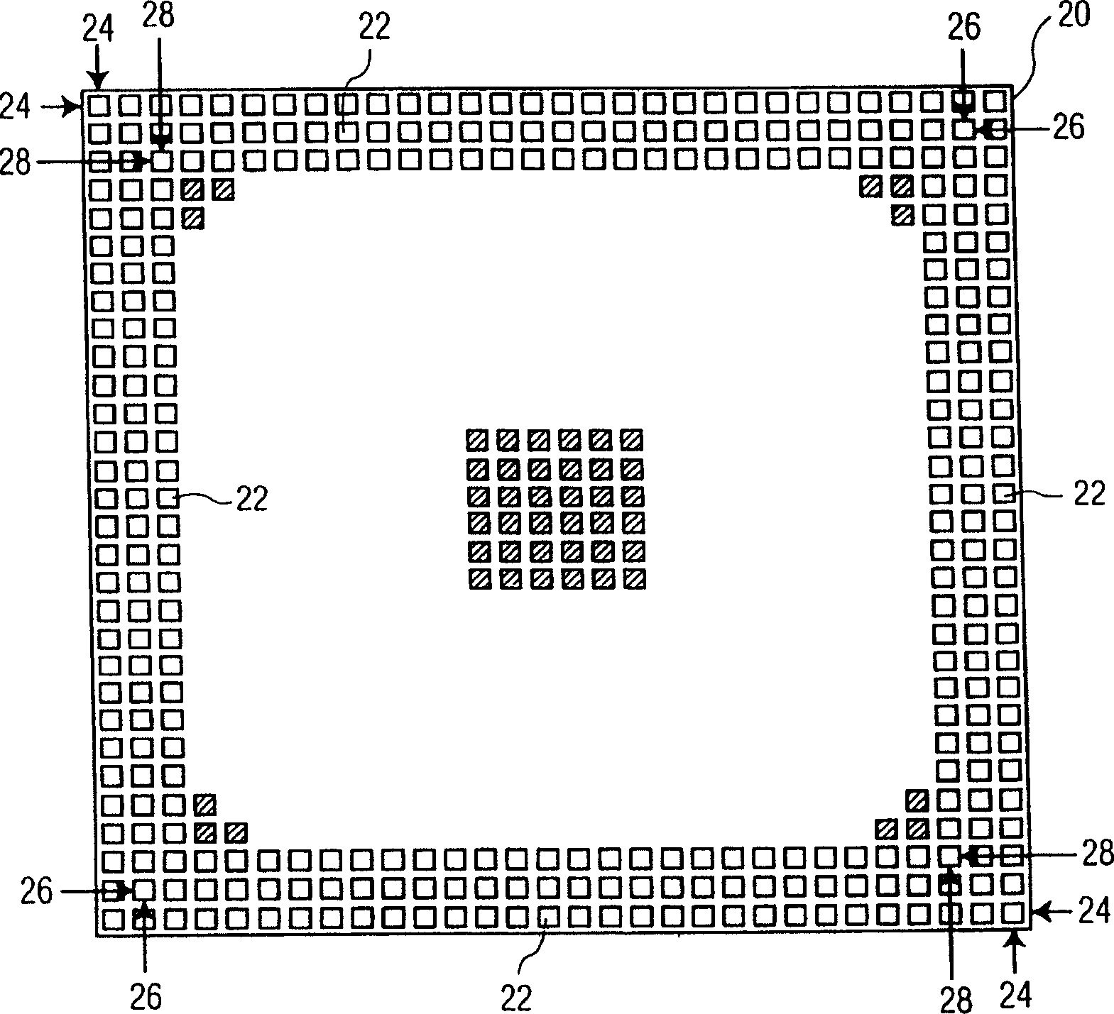
[0025] In accordance with one aspect of the present invention, a system, apparatus, and / or method is presented that provides an integrated circuit (IC) die bonding layout that allows for a minimum number of layers of a mating printed circuit board (PCB). The IC die bonding can be used for flip-chip, such as flip-chip ball grid array (BGA) applications.
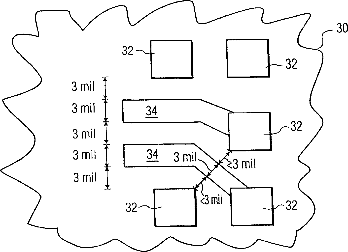
[0026] In one form thereof, this aspect takes into account the routing capabilities of the PCB and spaces every other row of bonding pads such that bonding pads from every other row and in relation to Two wires are routed between the outer row of bonding pads. This provides staggered spacing for the bond pads. At the same time, according to the principle of the present invention, there are many ways to realize the staggered spacing of the bonding pads, image 3 , 4 Several approaches and their corresponding pitches are shown in and 5.
[0027] When routing between pads on the same layer of the mating PCB is employed, pitch ...
PUM
 Abstract
Description
Claims
Application Information
 - R&D Engineer
- R&D Manager
- IP Professional
- Industry Leading Data Capabilities
- Powerful AI technology
- Patent DNA Extraction
Browse by: Latest US Patents, China's latest patents, Technical Efficacy Thesaurus, Application Domain, Technology Topic, Popular Technical Reports.
© 2024 PatSnap. All rights reserved.Legal|Privacy policy|Modern Slavery Act Transparency Statement|Sitemap|About US| Contact US: help@patsnap.com


