
Printed wiring board and semiconductor device

A printed circuit board, wiring technology, applied in the direction of printed circuit, printed circuit, printed circuit manufacturing, etc., can solve the problem of no solder mask and so on

Inactive Publication Date: 2005-06-22
MITSUI MINING & SMELTING CO LTD
View PDF0 Cites 11 Cited by
  • Summary
  • Abstract
  • Description
  • Claims
  • Application Information

AI Technical Summary

Problems solved by technology

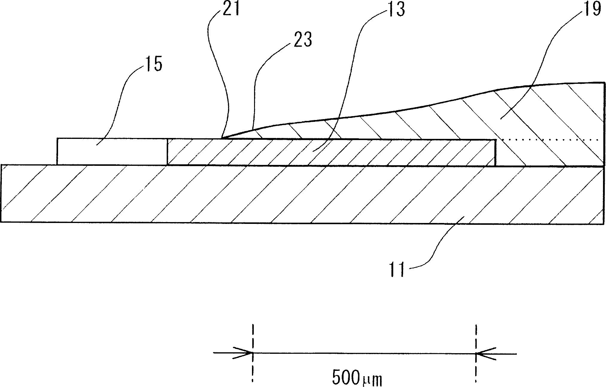
However, there is no description in this publication about the formation of the solder resist in the shape of a bevel towards the edge

Method used


Image

  • Printed wiring board and semiconductor device
  • Printed wiring board and semiconductor device
  • Printed wiring board and semiconductor device

Examples


Embodiment 1

[0071] A laminate comprising a polyimide film (available from Bbe industries, Ltd., Upilex S) having a thickness of 75 μm and an electrodeposited copper foil having a thickness of 18 μm was prepared.

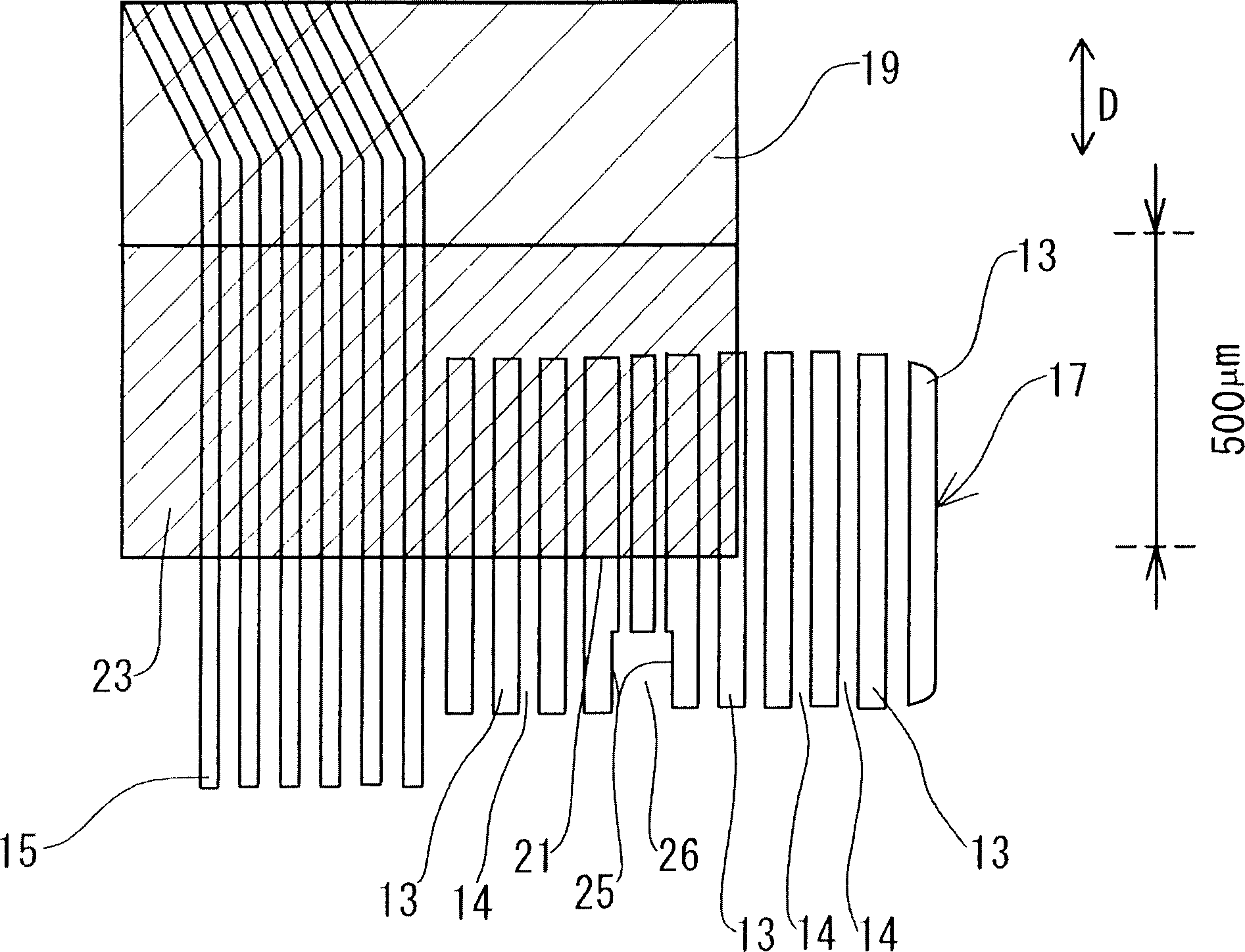
[0072] Such as figure 2 As shown, the surface of the electrodeposited copper foil of the laminate is coated with a photoresist material, and the photoresist material is exposed and developed to form a lead pattern and a filament pattern almost parallel to the lead pattern. Then, using the pattern thus formed as a masking material, the copper foil is selectively etched with an etching solution to form a predetermined wiring pattern. In the wiring pattern thus formed, such as figure 2 This dummy pattern shown consisting of a large number of filaments approximately parallel to the outer lead is formed on the outer lead side. The pitch of the outer leads was 80 μm (lead width: 40 μm, interval: 40 μm), and the interval between the outermost lead of the outer leads and the dummy p...

Embodiment 2

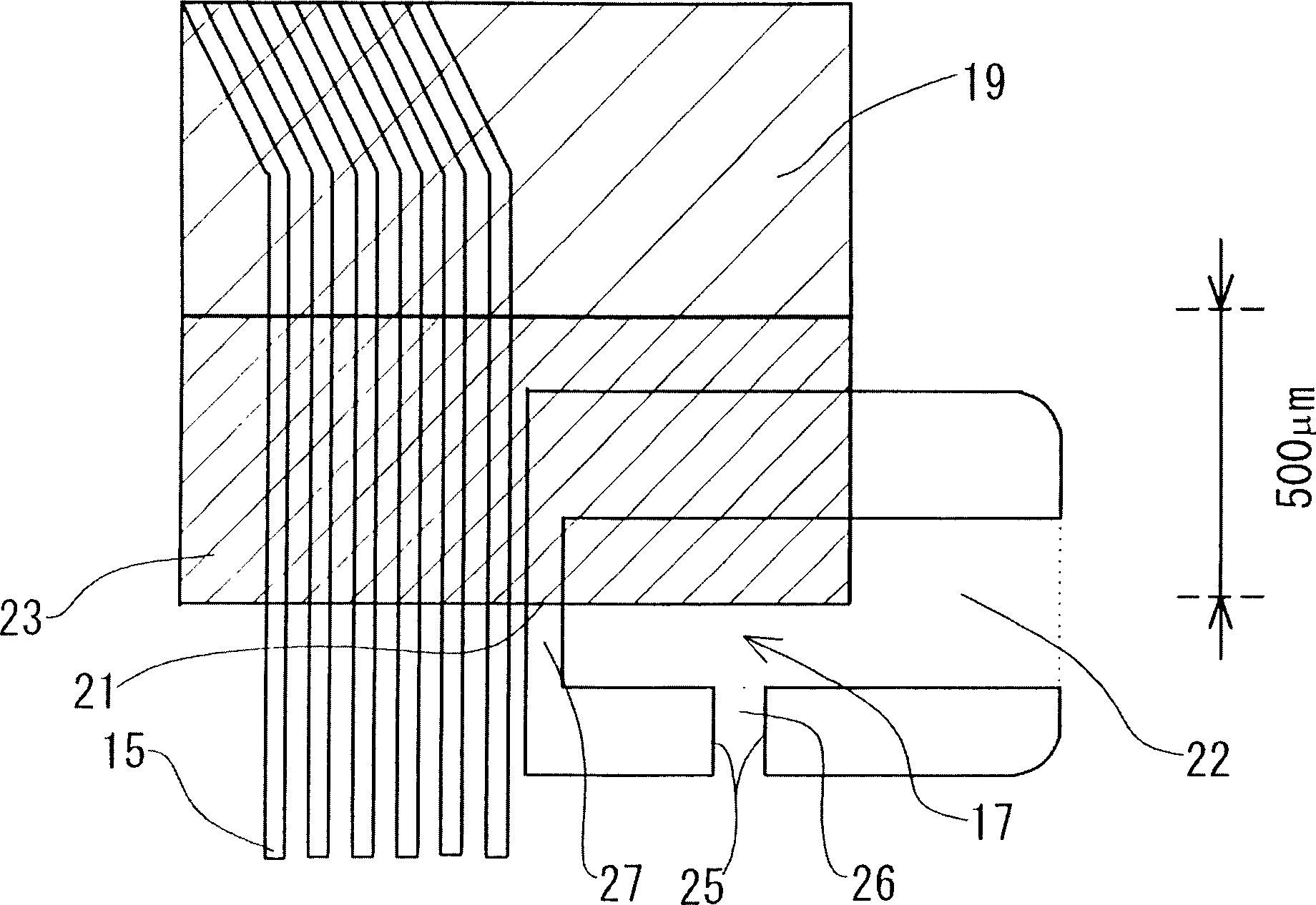
[0089] In addition to the shape of the dummy figure such as image 3 The membrane support was prepared in the same manner as in Example 1 except for the changes shown. That is, a dummy pattern is formed at a position 40 μm away from the edge of the wiring pattern 15 formed of a plurality of wirings formed approximately parallel to each other so that the outer peripheral metal edge 27 is parallel to the plurality of wirings of the wiring pattern 15 . This dummy pattern has a slit 22 formed in such a manner that a central portion of the dummy pattern is removed from the side not facing the wiring pattern 15 . In the dummy pattern, alignment recesses 26 are formed. The bottom of the depression 26 is connected to the cutout 22 and the peripheral metal edge 27 is discontinuous at the location of the depression 26 .

[0090] When observing the edge portion of the above-prepared solder resist layer having a slope length of 500 μm, the solder resist layer had a slope extending unifo...


PUM


Abstract

The invention discloses a printed wiring board which has a large number of wirings formed approximately parallel to each other, dummy patterns formed along the wirings, and a solder resist layer formed by coating the wirings and dummy patterns with a solder resist, the resist The solder coating thickness decreases toward the edge, wherein the dummy pattern has a solder resist coating thickness control area. The present invention also discloses a semiconductor device, which includes the above-mentioned printed circuit board and electronic components mounted on it. According to the present invention, the slope extending uniformly over the entire width of the solder resist can be formed at the edge portion of the solder resist.

Description

technical field [0001] The invention relates to a printed circuit board and a semiconductor device with a solder resist layer, wherein the coating thickness of the solder resist layer decreases toward the edge to form a bevel. More particularly, the present invention relates to a printed wiring board having a solder resist layer, wherein an edge portion of the solder resist layer has a bevel shape and the solder resist layer has a dummy pattern of a specific shape. Background technique [0002] For mounting electronic components, a carrier having a wiring pattern on the surface of an insulating substrate is used. The formation process of this carrier includes: forming a photosensitive resin layer (photosensitive resin layer) on the surface of a laminate (laminate) composed of an insulating base and a conductive metal; exposing and developing the photosensitive resin layer to form a desired pattern; using the thus formed The pattern of the conductive metal is selectively etc...

Claims


Application Information

Patent Timeline
Patent Type & Authority Applications(China)
IPC IPC(8): H05K3/28H05K1/02H05K3/34
CPCH05K1/0266H05K1/0271H05K3/3452H05K2201/09781H05K2203/0594H05K1/02H05K3/28
Inventor 藤井延朗
Owner MITSUI MINING & SMELTING CO LTD
Learn More