Eureka AIR delivers breakthrough ideas for toughest innovation challenges, trusted by R&D personnel around the world.

Method of selective laser crystallization and display panel manufactured by same method

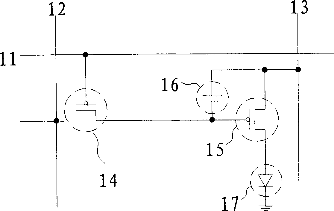
A display panel and light-emitting display technology, applied to light sources, electric light sources, static indicators, etc., can solve problems such as pulse omission, ripple defects, and electrical inhomogeneity

Active Publication Date: 2005-06-01
테스콤가부시키가이샤
View PDF0 Cites 4 Cited by
  • Summary
  • Abstract
  • Description
  • Claims
  • Application Information

AI Technical Summary

Problems solved by technology

Traditionally, excimer lasers are often used to convert amorphous silicon in the drive circuit area and active light-emitting display area into polysilicon. However, during the crystallization process using excimer lasers, laser pulse energy errors and pulse omissions are prone to occur, making crystallized crystals The grain size and grain boundary are irregular, so after the operating voltage is driven, the current obtained by each TFT is different, resulting in uneven electrical properties of the TFT when driving the active light-emitting display area, making the display prone to point defects or other ripple defects (Mura)

Method used


Image

  • Method of selective laser crystallization and display panel manufactured by same method
  • Method of selective laser crystallization and display panel manufactured by same method
  • Method of selective laser crystallization and display panel manufactured by same method

Examples


Embodiment Construction

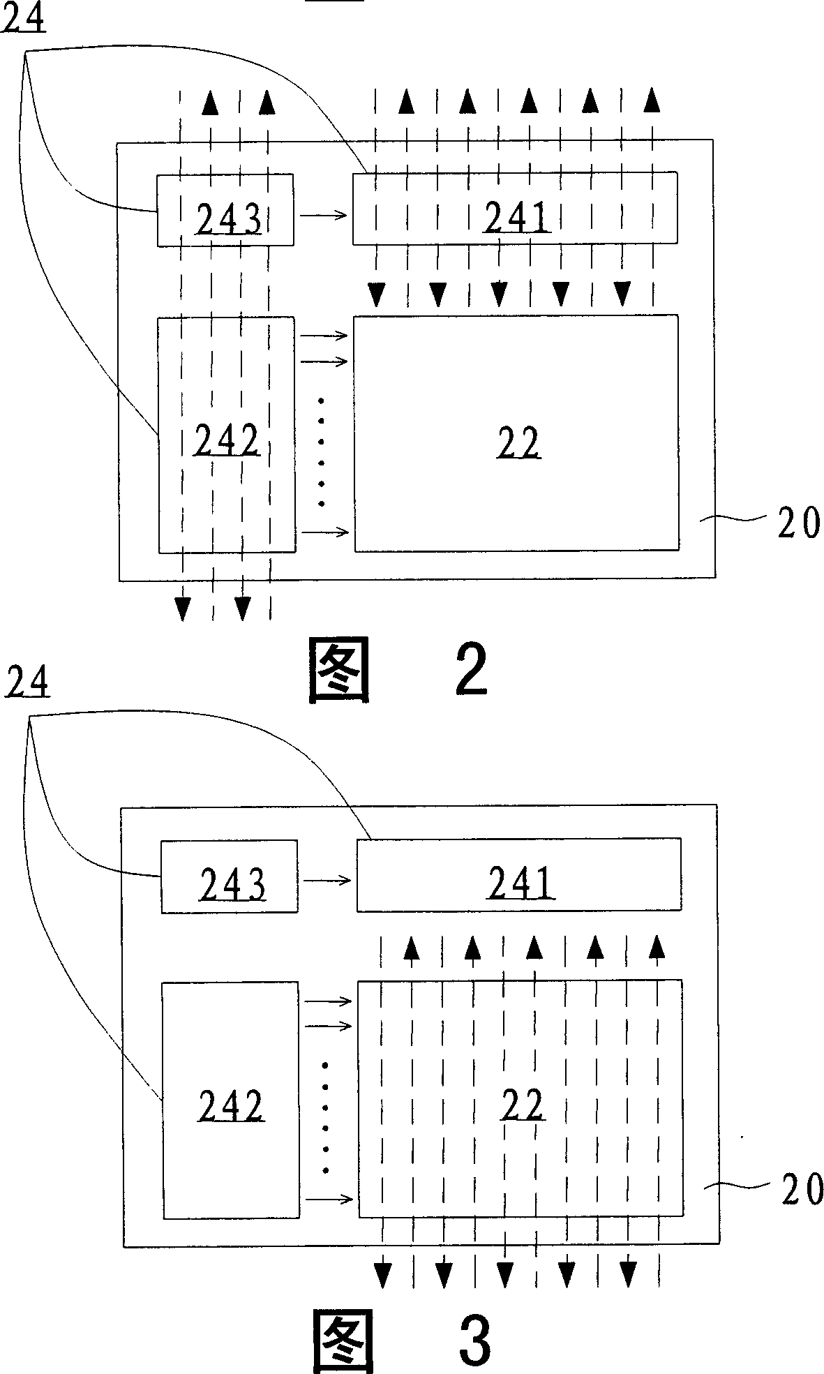
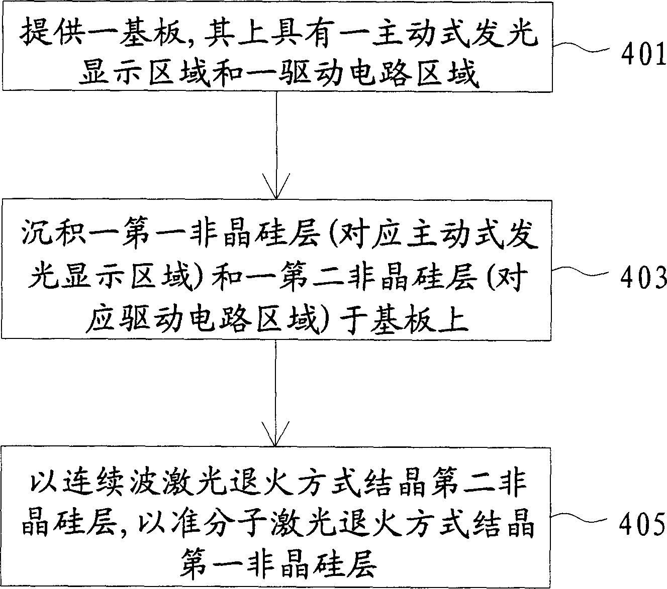
[0018] The present invention uses selective laser crystallization to crystallize the active light-emitting display area and the driving circuit area of ​​the display panel in different ways, so that the production of the display panel can increase the throughput and the driving circuit area has good performance. Carrier mobility (Mobility). Wherein, the polysilicon in the driving circuit region is formed by continuous wave laser annealing (Continuous Wave Laser Annealing; CW Laser Annealing). As for the polysilicon in the active light-emitting display area, a method with a larger tempering distance and less overlap can be used, such as an Excimer Laser Annealing (ELA) method. In this way, the grain size of the polysilicon layer in the driving circuit area is larger, and the grain boundaries are more regular, so that the electrical performance of the carrier mobility is better; while the grain size of the polysilicon layer formed in the active light-emitting display area is sma...


PUM

PropertyMeasurementUnit
Grainaaaaaaaaaa

Abstract

The display panel includes one substrate with one active light emitting display region and one circuit driving region; and one polysilicon layer formed on the substrate and with the first polysilicon layer arean and the second polysillicon layer area separately corresponding to the active light emitting display region and the circuit driving region, with the second polysillicon layer area having greater crystal grain size. The second polysillicon layer arean is formed in continuous wave laser annealing mode, while the first polysilicon layer arean is formed in excimer laser annealing mode.

Description

technical field [0001] The present invention relates to a display panel and a manufacturing method thereof, and in particular to a method for converting amorphous silicon of a display panel into polysilicon by selective laser crystallization and a display panel manufactured therefor. Background technique [0002] Organic Electroluminescence (Organic Electroluminescence) flat panel displays are current-driven components, and can be divided into passive matrix method and active matrix method according to the driving method. The active organic light emitting display (AMOLED) uses a thin film transistor (Thin Film Transistor, TFT) with a capacitive storage device to control the brightness grayscale performance of the organic light emitting device (OLED). [0003] Generally speaking, the production cost and technical threshold of passive organic light-emitting display (PMOLED) are low, but limited by the poor performance of the driving current, the resolution cannot be improved, ...

Claims


Application Information

Patent Timeline
IPC IPC(8): G09F9/00G09G3/30H05B33/10H05B33/12H05B44/00
Inventor 许忠义张志雄
Owner 테스콤가부시키가이샤
Why Eureka
Eureka Blog
Learn More