Semiconductor memory device

A storage device and semiconductor technology, applied in semiconductor devices, information storage, semiconductor/solid-state device manufacturing, etc., can solve problems such as difficult to obtain detection sensitivity, high-speed readout, and time-consuming

Inactive Publication Date: 2004-12-01
KK TOSHIBA
View PDF2 Cites 7 Cited by
  • Summary
  • Abstract
  • Description
  • Claims
  • Application Information

AI Technical Summary

Problems solved by technology

However, the level of the bit line at the time of data reading of the FBC memory must be lowered to suppress impact ionization, so that it is difficult to flow a large cell current, and it is difficult to obtain high detection sensitivity.
If a large cell current cannot flow, it takes time to charge and discharge the bit line connected to the drain of the memory cell, and high-speed reading cannot be performed.

Method used


Image

  • Semiconductor memory device
  • Semiconductor memory device
  • Semiconductor memory device

Examples


Embodiment Construction

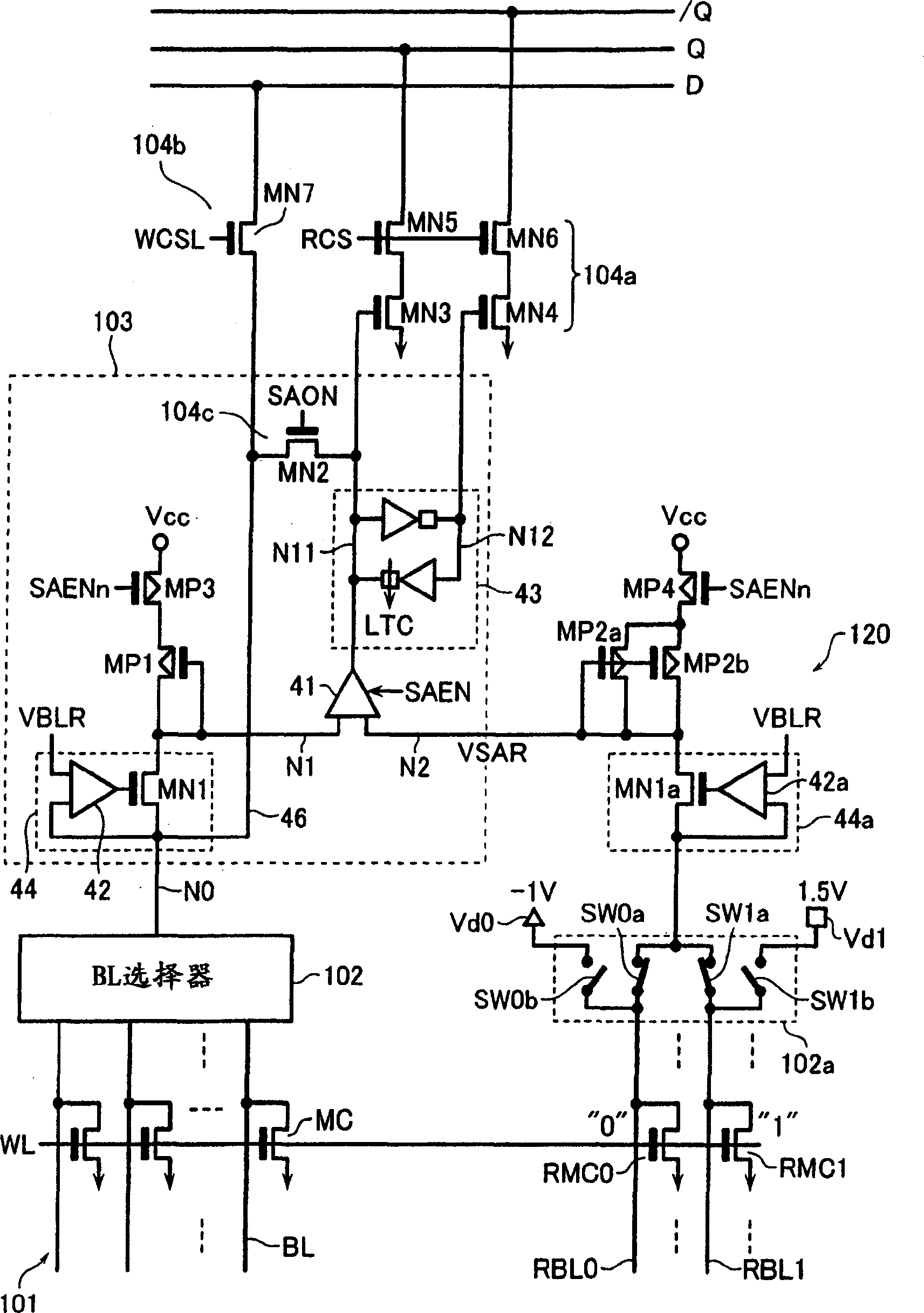
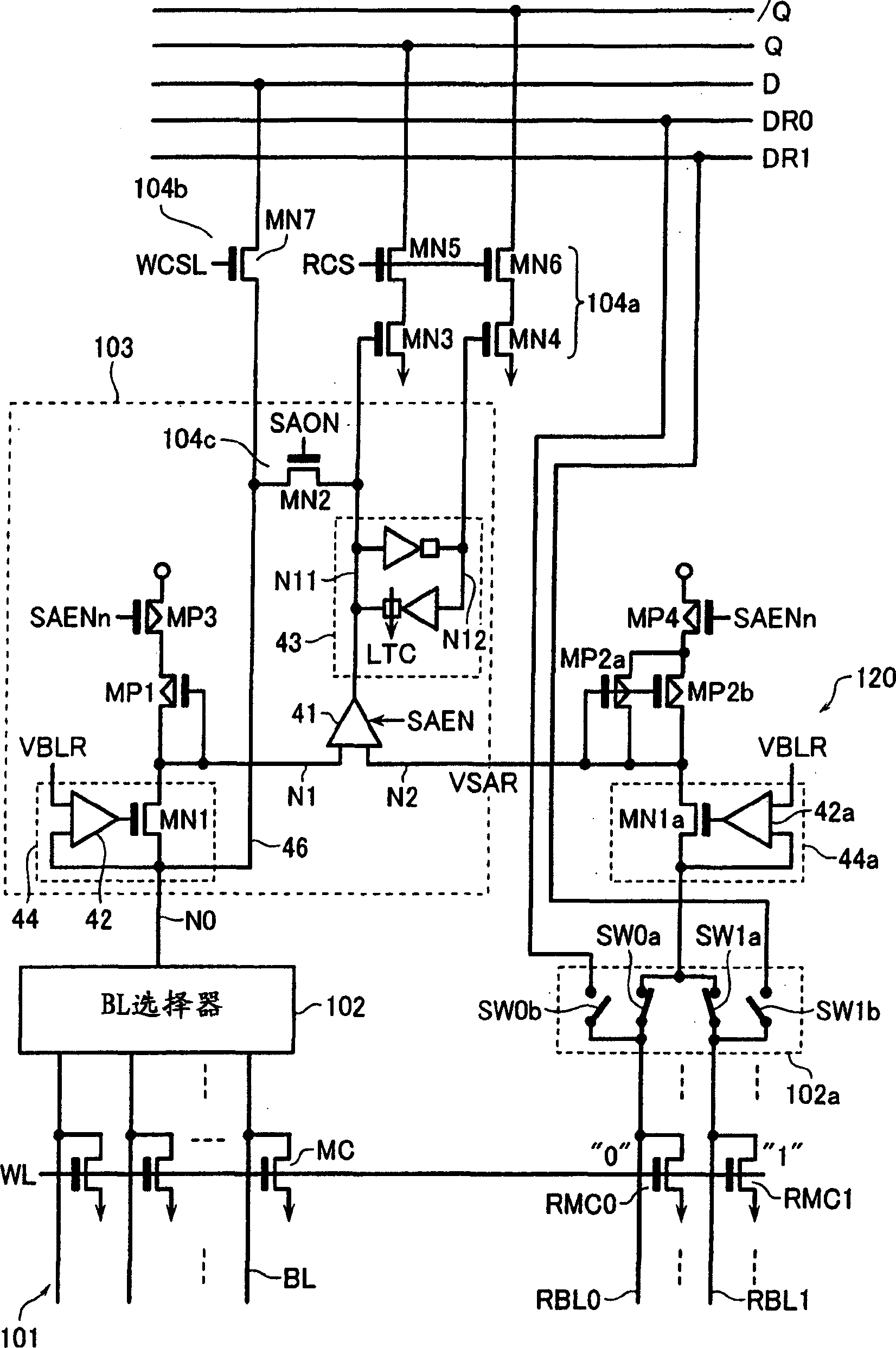
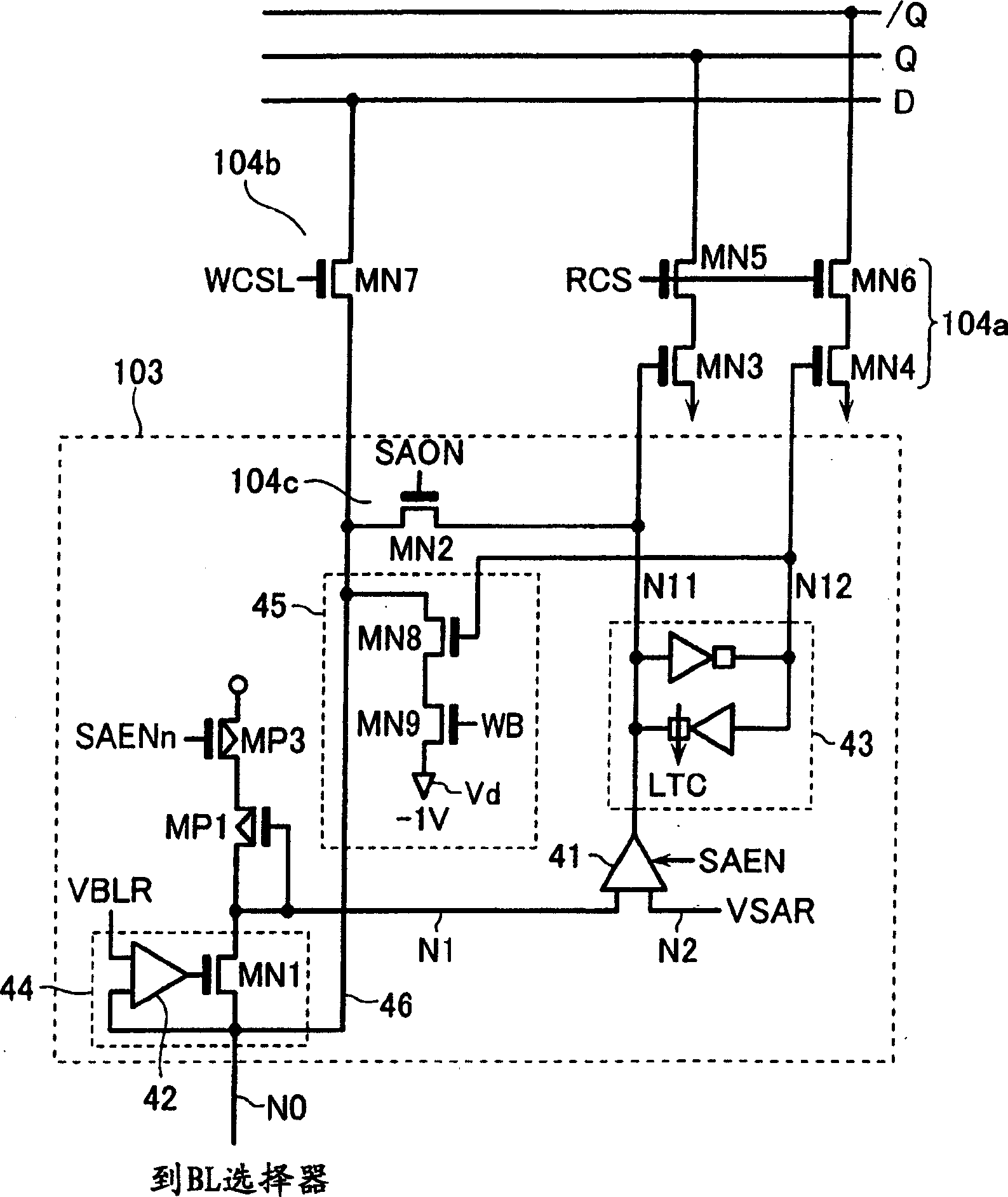
[0036] Hereinafter, embodiments of the present invention will be described with reference to the drawings.

[0037] First, the structure of the memory cell array of the FBC memory of the embodiment of the present invention will be explained. Figure 7 Is a plan view of the memory cell array, Figure 8 , Picture 9 with Picture 10 Respectively are Figure 7 Cross-sectional views along I-I', II-II' and III-III'.

[0038] N is formed on the surface of the P-type silicon substrate 10 + The surface of the molding layer 11 is covered with an insulating layer 12 such as a silicon oxide film. As a result, a P-type silicon layer 13 which is an active layer separated from the substrate 10 is formed on the insulating layer 12. After forming the gate 15 and the N-type source and drain diffusion layers 16a, 16b on the silicon layer 13 of this SOI substrate, a memory cell MC composed of an N-channel MOS transistor with a floating body is formed.

[0039] Like the bit line (BL) 19 to be formed ...


PUM


Abstract

A semiconductor memory device includes: a device substrate having a semiconductor layer separated by a dielectric layer from a base substrate; a memory cell array having a plurality of memory cells formed and arranged on the semiconductor layer of the device substrate, each the memory cell having a MOS transistor structure with a body in an electrically floating state to store data based on a majority carrier accumulation state of the body; and a sense amplifier circuit configured to read out data of a selected memory cell in the memory cell array to store the read data in a data latch, then transfer the read data to an output circuit and write back the read data into the selected memory cell.

Description

Technical field [0001] The present invention relates to a semiconductor storage device having a memory cell with a transistor / cell structure formed on an SOI substrate. Background technique [0002] Recently, in order to replace the existing DRAM, a semiconductor memory capable of dynamic storage with a simpler cell structure has been proposed (refer to Non-Patent Document 1). The memory cell is composed of one transistor having a floating body (channel body) formed on an SOI substrate. This memory cell sets the state where the excess majority carriers are stored in the main body to the first data state (for example, data "1"), and the state where the excess majority carriers are released from the main body to the second data state ( For example, data "0"), for binary storage. [0003] In the following, this memory cell is called "FBC" (Floating Body Cell), and the semiconductor memory using FBC is called "FBC memory". FBC memory, like normal DRAM, does not use capacitors, the st...

Claims


Application Information

Patent Timeline
Patent Type & Authority Applications(China)
IPC IPC(8): H01L27/108G11C7/06G11C11/401G11C11/404G11C11/406G11C11/4091G11C16/00H01L21/8242
CPCH01L29/7841G11C11/406G11C11/4091G11C2211/4016G11C7/062G11C2211/4068G11C2207/065G11C7/067G11C7/1051
Inventor 池桥民雄大泽隆藤田胜之
Owner KK TOSHIBA
Why Eureka
Try Eureka