


Quick Research
Generate reliable direction feasibility study reports for your R&D in just a few steps.

Technical Q&A
Discover and master advanced knowledge NOW. Basics, ideas, possibilities, all at once.

Find Solutions
As an expert in R&D theories, this can generate solutions to your technical problems instantly.

Evaluate Feasibility
Analyze your overall solution with one click, know your potential R&D risks in advance.

Monitor Landscape
Get weekly tech updates, stay abreast of the latest tech innovations and key insights.
Defect examining method of gray mask and mfg. method thereof
A technology for gray-tone masking and defect inspection, which is applied to the photolithographic process of patterned surfaces, semiconductor/solid-state device manufacturing, and illuminated markings, etc., which can solve short circuits, difficult correction accuracy, and lower gray-tone mask yields And other issues
- Summary
- Abstract
- Description
- Claims
- Application Information
AI Technical Summary
Problems solved by technology
Method used
Image

Examples
Embodiment 1
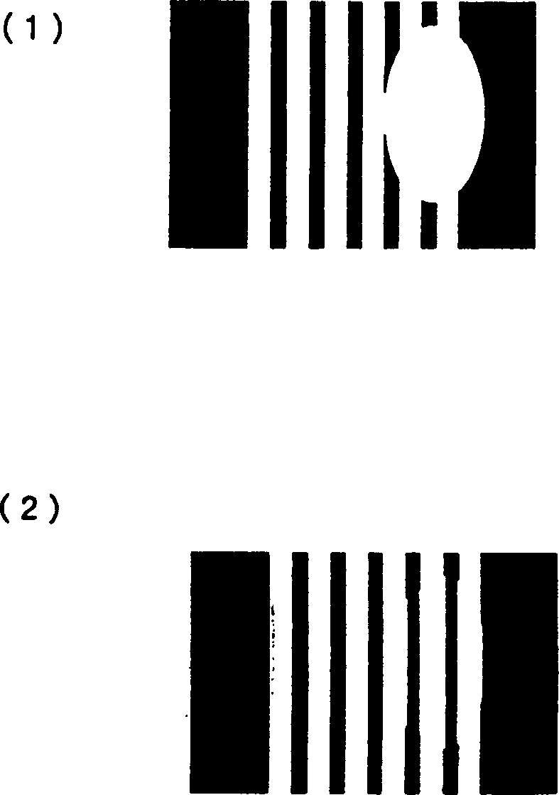
[0033] (Example 1): Inspection of gray tone part
[0034] Use a gray tone mask to transfer the pattern onto the resist film, and use the simulation method to obtain the film thickness of the developed resist film (when the resist film corresponding to the light-shielding part is set to 100 and the gray tone corresponding resist film). The resist film corresponding to the gray tone part is ideally 40-50. In the defect inspection process of the conventional gray tone area, the defect threshold value is set as Defect inspection was performed with the black defect side being 50 and the white defect side being 40.
[0035] Then, defect inspection was performed by setting the defect threshold to 50 on the black defect side and 30 on the white defect side. As a result, the gray tone mask can be manufactured with high yield, and the defect of the TFT substrate does not occur.
Embodiment 2
[0036] (Example 2): Correction of gray tone mask
[0037] Such as figure 1 As shown in (1), in the gray tone part where a part of the pattern is missing and a white defect occurs, such as figure 1 As shown in (2), a correction pattern (referred to as a correction pattern on the white defect pattern side in the present invention) as a white defect pattern is applied by laser CVD in accordance with a normal white defect side defect threshold. The same defect inspection was performed on the gray tone portion of the gray tone mask corrected in this way using the same defect threshold as described above, and as a result, the defect level was included in the allowable range.
PUM
 Abstract
Description
Claims
Application Information
 - R&D Engineer
- R&D Manager
- IP Professional
- Industry Leading Data Capabilities
- Powerful AI technology
- Patent DNA Extraction
Browse by: Latest US Patents, China's latest patents, Technical Efficacy Thesaurus, Application Domain, Technology Topic, Popular Technical Reports.
© 2024 PatSnap. All rights reserved.Legal|Privacy policy|Modern Slavery Act Transparency Statement|Sitemap|About US| Contact US: help@patsnap.com