
Image sensor packaging method

A technology of image sensors and circuit substrates, applied in the direction of electric solid-state devices, semiconductor devices, radiation control devices, etc., can solve problems such as warping of grains or products, peeling of two-layer PCB boards, poor product reliability, etc., and achieve packaging volume The effect of reducing and simplifying mechanical equipment and improving product reliability

Inactive Publication Date: 2004-02-18
王鸿仁
View PDF0 Cites 12 Cited by
  • Summary
  • Abstract
  • Description
  • Claims
  • Application Information

AI Technical Summary

Problems solved by technology

[0004] (2) Figure 15 The shown plastic substrate assembly (PLCC) needs to be injected into the side wall 80a of the PCB board (Pre-mold), and the substrate 80b of the L / F plastic injection assembly (KLCC) needs to be injected with the lead frame. These two assembly methods require separate injection Mold, so the manufacturing process is complicated and the cost is only lower than that of ceramic assembly, and the poor heat dissipation of the two packages may easily cause warpage and moisture problems of the die or product, resulting in poor reliability of the product
[0005] (3) In the plastic substrate assembly (PLCC) shown in FIG. 16 , the substrate is mainly formed by stacking and gluing another PCB board above the PCB board 81b with circuit wiring, so its manufacturing process is more complicated, and will cause two Layer PCB boards will peel off due to gluing flaws
[0006] (4) Plastic substrate assembly (PLCC) and L / F plastic injection assembly increase the process of leadframe (Leadfram) 81, 82. Although it can be automated and mass-produced, it is necessary to consider the precision of the leadframe to overcome the reliability problem of wire bonding. , and it is not easy to apply to high I / O chip packaging
[0007] Based on the aforementioned assembly technologies, wire bonding is required. In addition to adding equipment, it is difficult to improve production efficiency, and the final package size is too large due to the limited requirements of the substrate. Therefore, for mobile phones, PDAs, network cameras, etc. Such mobile electronic products are still too large. Therefore, the current trend of assembly technology is towards flip chip (Flip chip) packaging. This kind of process requires long bumps (Bump) to be set on the wafer (Wafer), and then bonded to the substrate Therefore, the top surface of the die needs to face the substrate, which limits the prerequisites for the sensing area of ​​the image sensor to be open. Therefore, although the flip chip has the best electrical characteristics, good heat dissipation of the die and a smaller package size, the application of this technology in image sensors is still difficult. As shown in FIG. 18 , it is an existing flip-chip assembly structure 9 for image sensors, and the inner surface of the glass plate 91 above it uses photomask etching technology to construct a circuit 910. Therefore, the manufacturing process is quite complicated, and the optical characteristics may be affected by the glue filling between the glass plate and the die, or the die may be affected by moisture, which may affect the reliability of the packaging product.

Method used


Image

  • Image sensor packaging method
  • Image sensor packaging method
  • Image sensor packaging method

Examples


Embodiment Construction

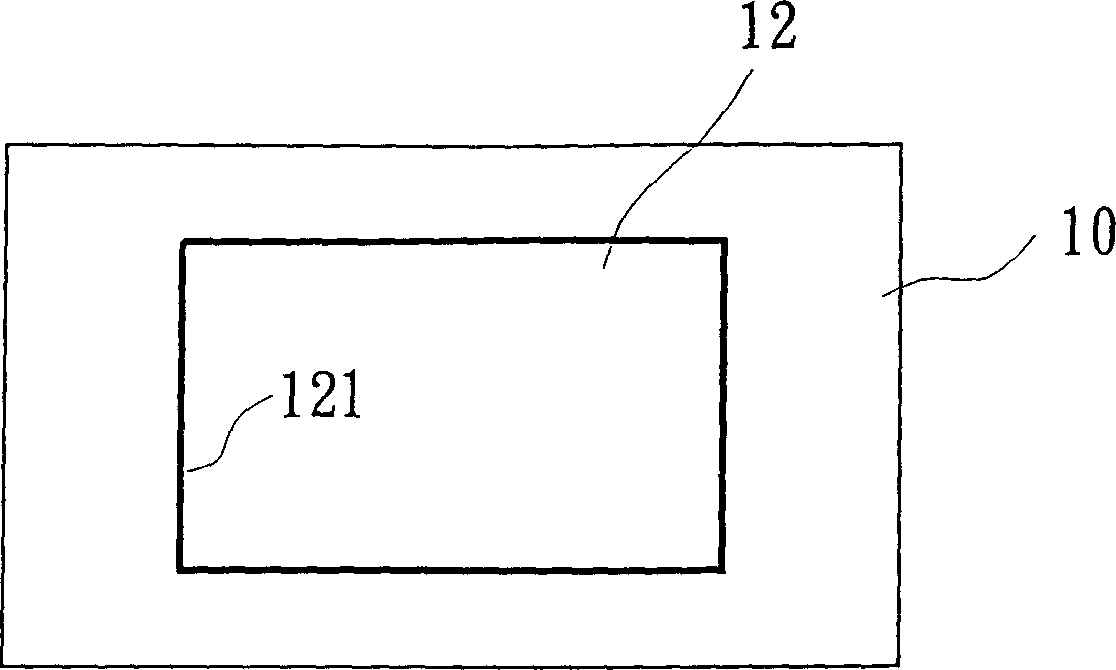
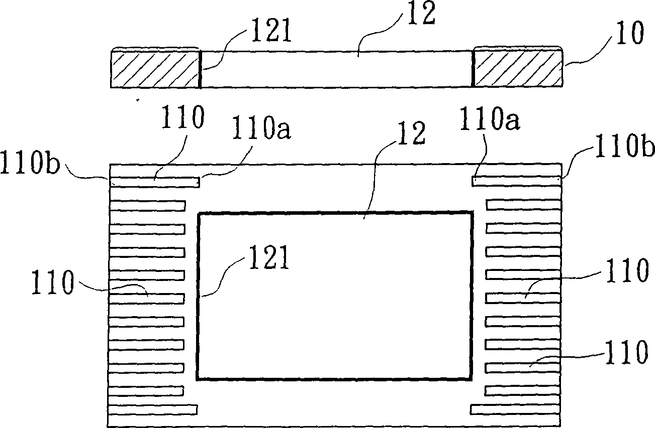
[0042] Cooperate Figure 1 to Figure 8 Shown illustrates the flow process of the image sensor packaging method of the present invention, including:

[0043] Step 1: If figure 1 , figure 2 As shown, a window 12 is opened on the surface of a PCB circuit substrate 10 with a conductive layer 11 on one surface, and the window penetrates to another corresponding surface of the PCB circuit substrate. The size of the window is close to the size of the sensing area of ​​an image sensor (such as Figure 5 21), and the walls of the window are coated with a shield 121 such as a solder mask or a gold-plated cover to prevent the dust after substrate processing from falling onto the surface of the image sensor die.

[0044] Step 2: If image 3 As shown, the aforementioned PCB circuit substrate is subjected to photomask etching (Etching) so that the conductive layer forms a plurality of leads (Leads) 110 on the window side, and each lead is set to include two parts: an inner lead 110a and ...


PUM


Abstract

The method includes setting image transducer on a PCB circuit base board which has conductive layer and a window on one surface, making window specification similar to sensing size of transducer crystal grain, forming multipin on the conductive layer, coverting electric-connection media at weld pad position and partial pin, joining crystal grain with PCB circuit base board through SMT preparationto form electric-connection, cleaning surface of image transducer crystal grain to remove odd parts, using glass and glue to seal and cover crystal grain in crystal grain sensing region and filling glue material arround crystal grain and glass to form air tightness and to finish packaging.

Description

technical field [0001] The invention relates to a CMOS / CCD (complementary metal oxide semiconductor / charge or photoelectric coupling device) image sensor packaging method. Background technique [0002] Common image sensor (Image sensor) IC assembly technology is ceramic assembly (CLCC), Figure 15 , plastic substrate assembly (PLCC) shown in Figure 16, and L / F plastic injection assembly (KLCC) shown in Figure 17. The main common feature of these assembly technologies is that the die is placed in the die pad and then wired (Wire bonding), however, under the guidance of wide application fields of image sensors and general consumer electronics products, the assembly cost and the size of the assembly are becoming more and more strict. Therefore, the aforementioned assembly technology has the following problems; [0003] (1) The production of substrate firing technology required for ceramic assembly (CLCC) does not easily lead to high assembly costs, and is usually only used in p...

Claims


Application Information

Patent Timeline
Patent Type & Authority Applications(China)
IPC IPC(8): H01L21/50H01L21/98H01L27/146H01L27/148
CPCH01L2224/48091
Inventor 王鸿仁
Owner 王鸿仁
Learn More