Light emitting diode

A technology of light-emitting diodes and electrodes, applied in electrical components, circuits, semiconductor devices, etc., can solve the problems of sudden increase, increase in forward voltage of components, difficult activation of impurities, etc., and achieve the effect of reducing light absorption area and improving brightness

Inactive Publication Date: 2003-08-20
EPITECH +1
View PDF0 Cites 6 Cited by
  • Summary
  • Abstract
  • Description
  • Claims
  • Application Information

AI Technical Summary

Problems solved by technology

Please refer to Figure 4 , if gallium arsenide is used as image 3 The material of the p-type ohmic contact layer 22 in the structure, then when the light-emitting wavelength of the active region is shorter than 870nm, the light absorption of the gallium arsenide material will increase sharply, which will make the aluminum gallium indium phosphide diode (wavelength between 550nm to 680nm) Between) the light output intensity is greatly attenuated
In addition, if gallium phosphide or gallium arsenide phosphide is used as image 3 When the material of the p-type ohmic contact layer 22 is used in the structure, although the energy gap of this two-term material is larger than that of gallium arsenide, and the amount of photons absorbed in the active region is less, its impurity activation is not easy, and the p-type concentration is often not high, which will It makes it difficult for the light-transmitting conductive oxide electrode layer 24 and the p-type ohmic contact layer 22 to form a good ohmic contact, so that the forward voltage of the element is greatly increased, and the application of the element is thus limited.

Method used


Image

  • Light emitting diode
  • Light emitting diode
  • Light emitting diode

Examples


Embodiment Construction

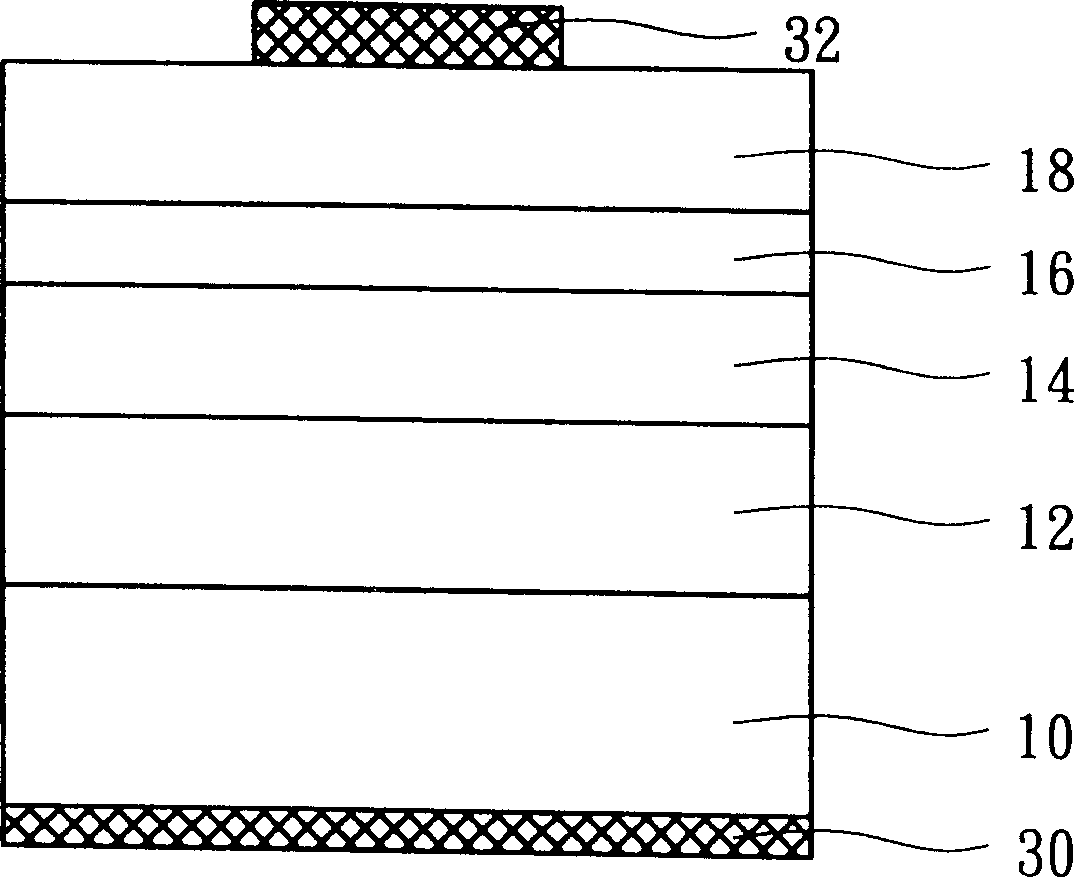
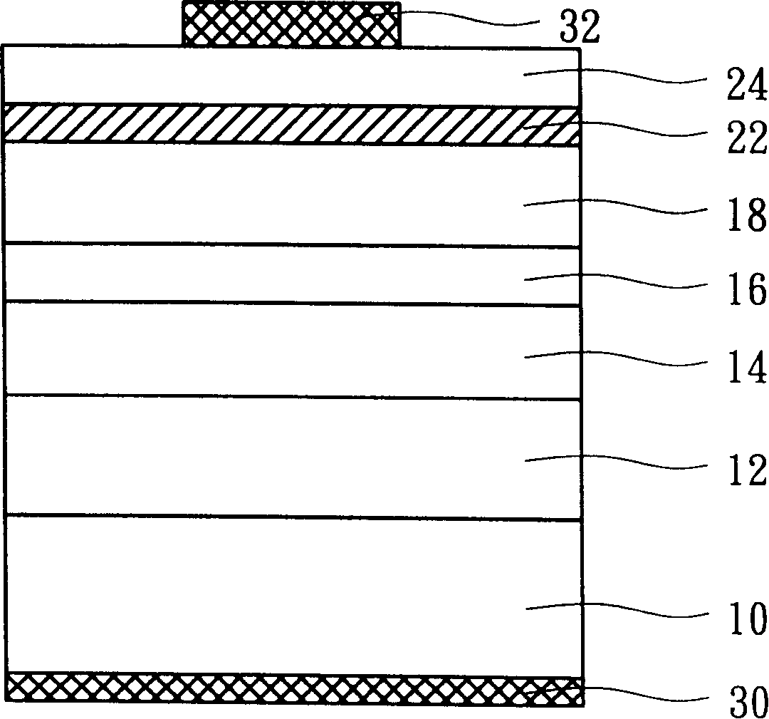
[0020] In the known technology, in order to prevent the photons emitted by the active region from being blocked by the front p-type metal, a gallium phosphide or aluminum gallium arsenide current dispersion layer with a thickness of tens of micrometers must be used to make the light emitting diode have a large current dispersion. However, growing a current spreading layer with a thickness of tens of micrometers is not only costly but also time-consuming. Therefore, a high-conductivity and high-transmittance oxide electrode (such as: indium tin oxide) is proposed in the known technology to enhance the current spreading ability. In order to form good ohmic characteristics between the conductive oxide electrode and the semiconductor, the known technology uses p-type gallium arsenide as the material of the ohmic contact layer, but because the energy gap of gallium arsenide is too small, it is easy to absorb photons emitted by the active region, Therefore, the effect of enhancing th...


PUM


Abstract

The present invention is one kind of high-brightness light-emitting diode. It has ohmic contact layer of p-type GaInP or oxide electrode contact layer of short-period superlattice thin layer with 10 to the power 18 / cm -3 over n-type or p-type doping density. The oxide electrode contact layer made of the special material has the In component regulated properly and thus light absorption amount, greatly raised p-type carrier density, raised light-emitting diode brightness and reduced forward voltage drop. In addition, the present invention discloses one oxide electrode contact layer with nettedor column pattern to expose partial current dispersing layer and this can reduce light absorbing area and raise the output light strength of the light-emitting diode without affecting the contact resistance and forward voltage.

Description

technical field [0001] The present invention relates to a light emitting diode (Light Emitting Diode; LED) structure, in particular to a light emitting diode structure capable of improving brightness. Background technique [0002] At present, light-emitting diodes are widely used in daily life because of their low production cost, low production difficulty, light weight, easy installation, and good development, such as electronic signage, indicator lights, and sensors. Even so, it is still a long-awaited goal to effectively further improve the luminous efficiency of light-emitting diodes. [0003] figure 1 Shown is a cross-sectional view of a known aluminum gallium indium phosphide (AlGaInP) light emitting diode. Please refer to figure 1 Generally, the aluminum gallium indium phosphide light-emitting diode forms an epitaxial structure on a substrate 10 made of n-type gallium arsenide by metal organic chemical vapor deposition (MOCVD: Metal Organic Chemical Vapor Depositio...

Claims


Application Information

Patent Timeline
IPC IPC(8): H01L33/10H01L33/40
Inventor 陈锡铭汪信全
Owner EPITECH
Why Eureka
Try Eureka