Multiple electrode array and manufacturing method

A technology of multi-electrode array and manufacturing method, which is applied in the field of multi-electrode array, can solve the problems of non-productization, large brain tissue damage, and difficulty in manufacturing density, and achieve easy implementation, high reliability and mechanical strength, and eliminate the need for soldering. The effect of line craft

Inactive Publication Date: 2006-11-22
INSITUTE OF BIOPHYSICS CHINESE ACADEMY OF SCIENCES
View PDF0 Cites 0 Cited by
  • Summary
  • Abstract
  • Description
  • Claims
  • Application Information

AI Technical Summary

Problems solved by technology

[0003] In 1981, American scientist Kruger et al. used ceramic materials to fix multiple microelectrodes on a grid with a spacing of 250 microns to form a multi-electrode array. This method is inefficient, and the length and parallelism of electrodes are not easy to control.
Afterwards, various improved multi-electrode array manufacturing methods appeared. For example, the electrode array of Utah University uses a dicing knife to directly carve a plurality of electrode tips on a silicon substrate, and then makes finished products through processes such as insulation and wire bonding. The problem with the method is that the size of the electrode tip cannot be made too thin, and the electrode that is too thick will cause great damage to the brain tissue, and it is also difficult to manufacture a high-density multi-electrode array
In addition, there are planar integrated circuit manufacturing processes such as photolithography and ion sputtering to make sheet-like multi-electrodes, and then laminated to form a multi-electrode array, such as the electrode array of the University of Michigan in the United States, but this type of electrode array is in terms of comprehensive performance. Still needs to be improved, and it has not yet been commercialized

Method used


Image

  • Multiple electrode array and manufacturing method
  • Multiple electrode array and manufacturing method
  • Multiple electrode array and manufacturing method

Examples


Embodiment

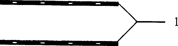
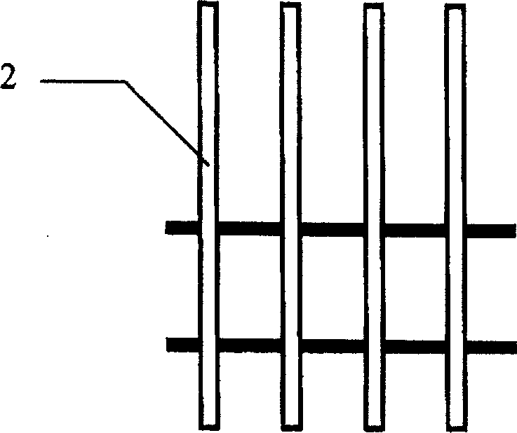
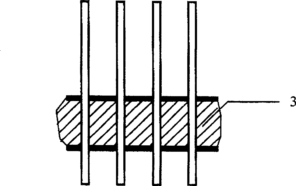
[0045] see Figure 1 (a) ~ Figure 1 (f) , Take two pieces of brass with a thickness of 0.05 mm, laser drill a 10×10 array of micro-holes with a diameter of 30 μm and a hole spacing of 200 μm. The two micro-hole array thin plates 1 are horizontally separated by 1 mm and fixed. Take the steel wire 2 with a diameter of about 27 microns, straighten it and cut it into 100 steel wires 2 of 30 mm length, and insert the steel wire 2 into the micro holes of the two micro-hole array plates 1 with the tip of about 1 mm exposed. , The rear end is exposed to an appropriate length. Put the newly prepared denture tray resin 3 into the space between the two microporous array sheets 1 immediately. After 20 minutes, the resin 3 will solidify, pull out the steel wire 2. Peel off the two microporous array sheets 1, and trim the shape of the denture block A micro-hole array 4 with a hole diameter of about 25 microns, a hole depth of 1 mm, and a 10×10 can be obtained.

[0046] Prepare one hundred single...


PUM


Abstract

The invention relates to multi-electrode array technology, in particular to a multi-electrode array manufacturing method. A multi-electrode array of the present invention is composed of a microhole array, a single electrode and a fixed resin, and the single electrode is rectangular and placed in the vertical hole of the microhole array; the tail of the single electrode is longer than the head and extends horizontally. The head of the single electrode is pointed and extends out of the vertical holes of the microhole array; there is fixed resin above the part of the horizontal tail of the single electrode and the upper surface of the microhole array. The invention uses metal wires as electrodes, the electrodes can be made very thin, and the distance between the electrodes can also be very small. The position, angle, and length of the electrode are limited by using a microhole array with a certain depth, which is easy to realize. Directly use the tail end of the electrode wire as the lead wire, which saves the difficult wire welding process, and has high reliability and mechanical strength.

Description

Technical field [0001] The invention relates to a multi-electrode array technology, in particular to a method for manufacturing a multi-electrode array. Background technique [0002] The multi-electrode array is an array of multiple microelectrodes integrated on a substrate, and the multi-electrode array implanted in the cerebral cortex can read the detailed information of the neuronal group activity in the brain. In terms of basic neuroscience research, multi-electrode arrays have begun to become an important means of neural information detection. In medical applications, multi-electrode arrays have become the interface of neuroscience to medical applications. [0003] In 1981, American scientist Kruger et al. used ceramic materials to fix multiple microelectrodes on a grid with a pitch of 250 microns to form a multi-electrode array. This method is inefficient and difficult to control the length and parallelism of the electrodes. In the future, a variety of improved methods for ...

Claims


Application Information

Patent Timeline
Patent Type & Authority Patents(China)
IPC IPC(8): A61B5/00
Inventor 唐世明
Owner INSITUTE OF BIOPHYSICS CHINESE ACADEMY OF SCIENCES
Why Eureka
Try Eureka