FDSOI device and manufacturing method thereof

A device and slot filling technology, applied in the field of FDSOI devices and their manufacturing, can solve problems such as poor heat dissipation performance and affect device performance, and achieve the effects of simplifying production processes, improving device performance, and reducing production costs

Inactive Publication Date: 2022-07-29
锐立平芯微电子(广州)有限责任公司 +1
View PDF0 Cites 0 Cited by
  • Summary
  • Abstract
  • Description
  • Claims
  • Application Information

AI Technical Summary

Problems solved by technology

[0005] The purpose of the present invention is to provide a FDSOI device and a manufacturing method thereof, so as to solve the technical problem that the existing FDSOI device has poor heat dissipation performance and affects device performance

Method used


Image

  • FDSOI device and manufacturing method thereof

Examples


Embodiment 1

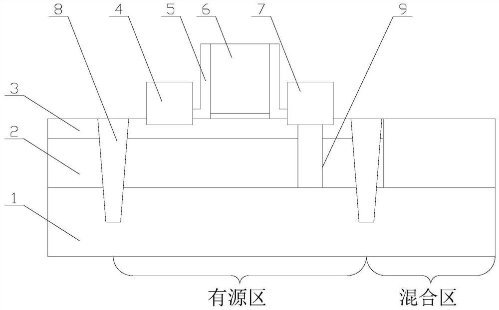
[0025] Example 1: as figure 1 As shown, an FDSOI device includes a substrate 1, a buried oxide layer 2 and a silicon-on-insulator layer 3 arranged in sequence from bottom to top, and a source electrode 4, a drain electrode 7 and a gate electrode 6 are provided on the top of the silicon-on-insulator layer 3 , the gate 6 is located between the source 4 and the drain 7, the sidewall of the gate 6 is provided with a sidewall 5, the gate 6 dielectric is silicon oxide, and the drain 7 is provided with a filling groove 9 with a width of 20nm, The filling trench 9 extends to the substrate 1 and is filled with silicon inside the filling trench 9 .

[0026] In this embodiment, since the thermal conductivity of silicon is better than that of silicon oxide in the buried oxide layer 2, the rate of heat transfer to the substrate 1 can be accelerated, and the rate of heat dissipation due to the hot carrier effect near the drain can be accelerated. Effectively improve the self-heating effect...

Embodiment 2

[0027] Embodiment 2: an FDSOI device, comprising a substrate 1, a buried oxide layer 2 and a silicon-on-insulator layer 3 arranged sequentially from bottom to top, and a source electrode 4, a drain electrode 7 and a gate electrode are provided on the top of the silicon-on-insulator layer 3 6. The gate 6 is located between the source 4 and the drain 7, a sidewall 5 is provided on the side wall of the gate 6, and the dielectric of the gate 6 is silicon oxide and high-K metal oxide arranged alternately from bottom to top. , the silicon oxide and the high-K metal oxide form a stacked structure, the drain 7 is provided with a filling groove 9 with a width of 100 nm, the filling groove 9 extends to the substrate 1, and the filling groove 9 is filled with silicon. High-K oxide has a high dielectric constant, which can increase the physical thickness of the gate dielectric while keeping the gate capacitance unchanged, so as to achieve the dual purpose of reducing gate leakage current a...


PUM

PropertyMeasurementUnit
Widthaaaaaaaaaa

Abstract

The FDSOI device comprises a substrate, a buried oxide layer and a silicon-on-insulator layer which are sequentially arranged from bottom to top, a source electrode, a drain electrode and a grid electrode are arranged on the top of the silicon-on-insulator layer, the grid electrode is located between the source electrode and the drain electrode, a side wall is arranged on the side wall of the grid electrode, a heat conduction area is further arranged on the drain electrode, and the heat conduction area is located between the source electrode and the drain electrode. The drain electrode is connected with the substrate through the heat conduction area. The drain electrode of the FDSOI device is directly connected with the substrate through the heat conduction area, so that heat generated by a hot carrier effect near the drain electrode can be transmitted to the substrate, the self-heating effect of the device can be effectively improved, and the performance of the device is improved; the filling groove is formed through synchronous etching by using the photomask used when the mixing area is etched, so that the production process can be simplified, the production efficiency can be improved, and the production cost can be reduced in the process of processing and forming the heat conduction area.

Description

technical field [0001] The invention belongs to the technical field of integrated circuit processing, and in particular relates to an FDSOI device and a manufacturing method thereof. Background technique [0002] In order to meet the requirement of scaling down the size of semiconductor devices in integrated circuit manufacturing, that is to say, the size of technology nodes has been continuously reduced. Although silicon-on-insulator technology (Fully-Depleated Silicon-On-Insulator, FDSOI, or FD-SOI) also provides another effective technical solution. A typical feature of the FDSOI-based process is that the wafers used have a layer of buried oxide (BOX) and an ultra-thin layer of silicon on insulator (SOI). Ultra-thin silicon-on-insulator (SOI) naturally limits the depth of the source-drain junction, and also defines the depletion region of the source-drain junction, which can improve short channels such as Drain induced barrier lowering (DIBL). effect, improve the sub-th...

Claims


Application Information

Patent Timeline
IPC IPC(8): H01L29/417H01L23/367H01L29/78H01L21/28H01L21/336
CPCH01L29/66477H01L29/401H01L29/78H01L29/4175H01L23/3677
Inventor 贺鑫叶甜春陈少民李彬鸿
Owner 锐立平芯微电子(广州)有限责任公司
Why Eureka
Try Eureka