
Ultra-wideband transparent wave absorber with simple double-layer structure

A double-layer structure, ultra-broadband technology, applied in the direction of antennas, electrical components, etc., can solve the problems such as the structure of the absorber that has not been proposed, and achieve a complex and changeable electromagnetic wave environment, good polarization stability, and small unit period. Effect

Pending Publication Date: 2022-07-22
NANJING UNIV OF SCI & TECH
View PDF2 Cites 0 Cited by
  • Summary
  • Abstract
  • Description
  • Claims
  • Application Information

AI Technical Summary

Problems solved by technology

[0005] Both of the above two schemes provide good absorbing performance in a wide bandwidth, but a simple and easy-to-process absorber structure is not proposed in the low frequency and widened bandwidth part.

Method used


Image

  • Ultra-wideband transparent wave absorber with simple double-layer structure
  • Ultra-wideband transparent wave absorber with simple double-layer structure
  • Ultra-wideband transparent wave absorber with simple double-layer structure

Examples


Embodiment

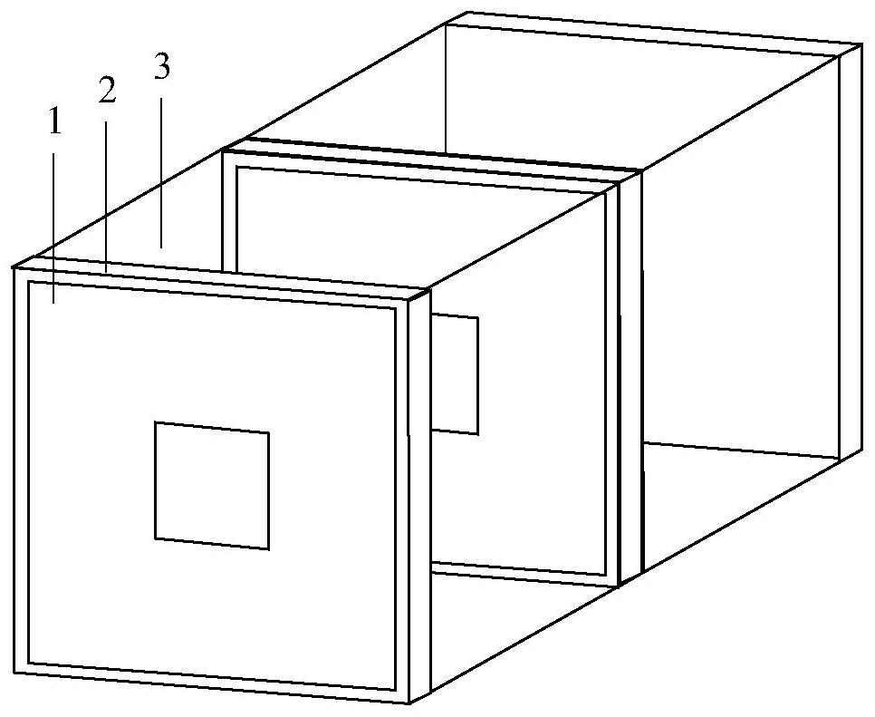
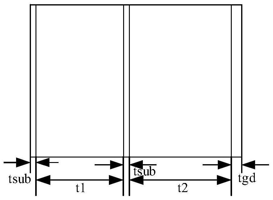
[0033] The invention provides an ultra-wideband transparent wave absorber with a simple double-layer structure, the specific structure of which is as follows: Figure 1-Figure 3 shown. The structural unit of the present invention is divided into three parts from top to bottom, the first part is the upper layer ITO film periodic structural unit and the corresponding glass substrate, the second part is the lower layer periodic structural unit with the same shape and the corresponding glass substrate, and the third part is the floor conductive film , the three parts are separated by two layers of air, the overall structure is as follows figure 1 shown.

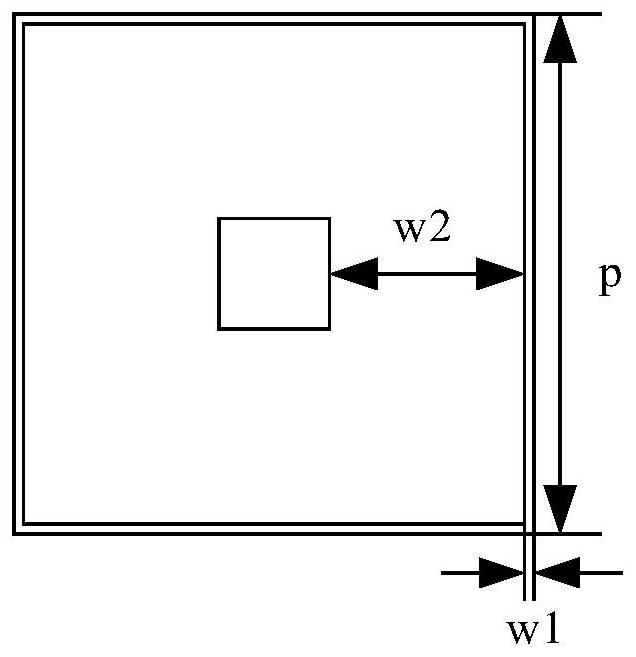
[0034] In this embodiment, the upper and lower layers of the conductive thin-film unit have the same structure, which is a square ring with a width of 3 mm, and the periodic unit size is 8 mm. The structure is as follows: figure 2 shown.

[0035] In this embodiment, the upper and lower dielectric substrates are made of quartz...


PUM

PropertyMeasurementUnit
angle of incidenceaaaaaaaaaa

Abstract

The invention discloses an ultra wide band transparent wave absorber with a simple double-layer structure, the structure is composed of a floor, an air layer, a glass substrate, an air layer and a glass substrate, the upper surface of each layer of glass substrate is attached with a same periodic structure formed by a transparent indium tin oxide film, and the floor also adopts a glass plate covered with a transparent ITO film. The wave absorber is simple and symmetrical in structure and easy to process, and due to the introduction of the air layer, not only is the weight of the wave absorber reduced, but also the relative bandwidth can reach 149%. For TE and TM vertical incident polarized waves, the wave absorbing rate of the wave absorber in the frequency band of 3-20.5 GHz is greater than 90%; for TE and TM inclined incident polarized waves, the wave absorber shows good wave absorbing performance with the wave absorbing rate larger than 80% within the range that the incident angle is smaller than 45 degrees.

Description

technical field [0001] The invention belongs to the technical field of broadband electromagnetic wave absorbers, in particular to a transparent wave absorber working in an ultra-wideband. Background technique [0002] The electromagnetic wave absorber is matched with the air through the input impedance, so that the plane wave will not be reflected on the surface of the absorber, and the incident electromagnetic wave is converted into other forms of energy through the loss mechanism such as the ohmic loss of the material, so as to achieve the effect of wave absorption. It can be used in military weapon systems, anechoic chambers, scientific or medical instruments and high-rise construction. At present, the vast majority of electromagnetic wave absorbers are optically opaque, which limits the application of wave absorbers to a certain extent. Therefore, on this basis, a transparent wave absorber is proposed to improve the security of wireless communication while ensuring It c...

Claims


Application Information

Patent Timeline
Patent Type & Authority Applications(China)
IPC IPC(8): H01Q17/00
CPCH01Q17/008
Inventor 仓佳星宗志园杨晓寒曹海若龙勋鹏吴文
Owner NANJING UNIV OF SCI & TECH
Learn More