Light emitting diode and preparation method thereof
A technology for light-emitting diodes and light-emitting layers, which is applied in the manufacture of semiconductor/solid-state devices, semiconductor devices, electrical components, etc., can solve the problems of insufficient stability of the water-oxygen environment of light-emitting diodes, and achieve good thermal stability, improved stability, and improved stability. The effect of gas barrier properties
- Summary
- Abstract
- Description
- Claims
- Application Information
AI Technical Summary
Problems solved by technology
Method used
Image
Examples
preparation example Construction
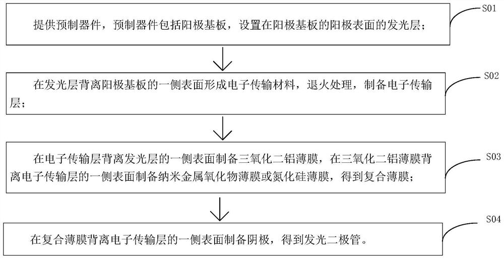
[0059] In a second aspect, the first aspect of the present application provides a method for preparing a light-emitting diode, comprising the following steps:
[0060] S10. Provide a prefabricated device, the prefabricated device includes an anode substrate, and a light-emitting layer disposed on an anode surface of the anode substrate.
[0061] In the embodiments of the present application, the prefabricated device is a local device that already has an anode substrate and after the light-emitting layer is prepared. In some embodiments, the prefabricated device further includes a hole functional layer between the anode and the light emitting layer. The hole functional layer includes at least one of a hole injection layer, a hole transport layer and an electron blocking layer.
[0062] In the examples of the present application, the preparation of the prefabricated device is not strictly limited, and can be prepared by conventional methods. In some embodiments, a method for p...
Embodiment 1
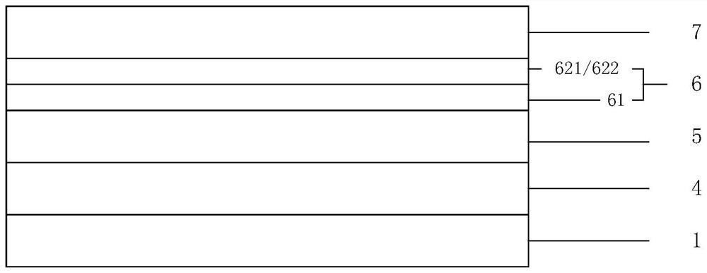
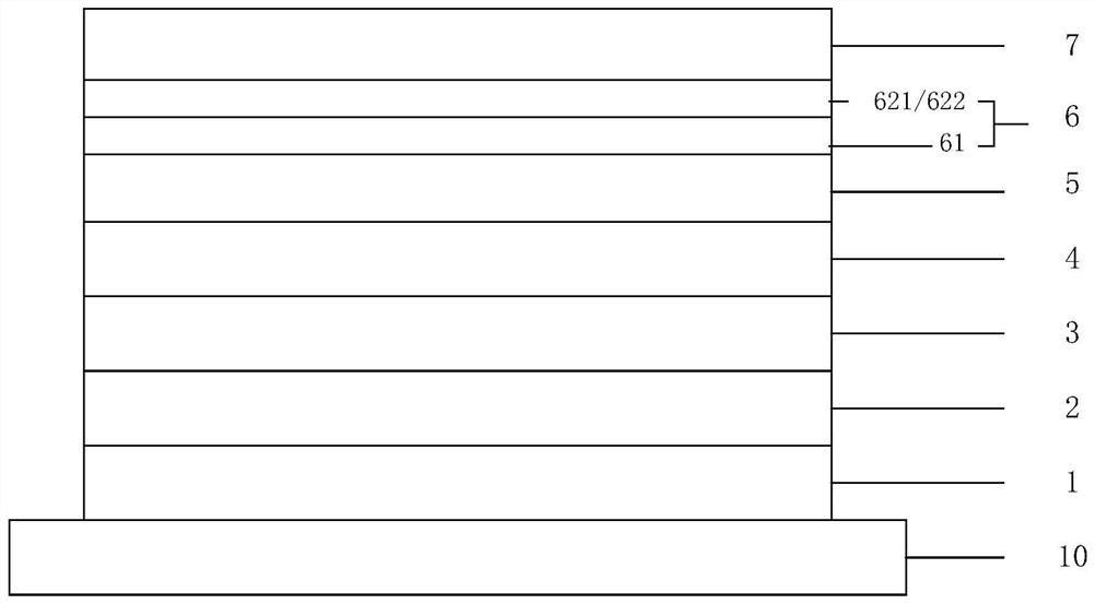
[0074] A quantum dot light-emitting diode with an upright structure is prepared by the following method:
[0075] Spin coating of PEDOT:PSS:s-MoO on ITO substrate 3 , and annealed in air to prepare a hole injection layer with a thickness of 30 nm;
[0076] In a nitrogen atmosphere, PVK was spin-coated on the hole injection layer and annealed at 140 °C to prepare a hole transport layer with a thickness of 20 nm;
[0077] CdSe@ZnS quantum dots were spin-coated on the hole transport layer to prepare a quantum dot light-emitting layer with a thickness of 40 nm;
[0078] MZO was spin-coated on the quantum dot light-emitting layer and annealed at 90 °C for 30 minutes to prepare an electron transport layer with a thickness of 50 nm;
[0079] 10nm Al was deposited on the electron transport layer by plasma enhanced atomic layer deposition (PEALD). 2 O 3 Thin films and 10nm TiO 2 film to obtain a composite film;
[0080] An Al electrode with a thickness of 85 nm was evaporated on ...
Embodiment 2
[0083] The difference from Example 1 is: 10nm TiO 2 The film was replaced with 10nm ZrO 2 film.
PUM
| Property | Measurement | Unit |
|---|---|---|
| Thickness | aaaaa | aaaaa |
Abstract
Description
Claims
Application Information
 - R&D Engineer
- R&D Manager
- IP Professional
- Industry Leading Data Capabilities
- Powerful AI technology
- Patent DNA Extraction
Browse by: Latest US Patents, China's latest patents, Technical Efficacy Thesaurus, Application Domain, Technology Topic, Popular Technical Reports.
© 2024 PatSnap. All rights reserved.Legal|Privacy policy|Modern Slavery Act Transparency Statement|Sitemap|About US| Contact US: help@patsnap.com


