Image processing-based method for predicting wire roughness of whole surface of monocrystalline silicon wafer cut by fretsaw

A monocrystalline silicon wafer and image processing technology, applied in the field of mechanical processing and manufacturing, can solve the problems of reducing the duration of minority carriers, increasing manufacturing costs, surface/subsurface damage, etc., and achieve the effect of shortening the time of manual measurement

Pending Publication Date: 2022-06-17
CHONGQING UNIV
View PDF0 Cites 0 Cited by
  • Summary
  • Abstract
  • Description
  • Claims
  • Application Information

AI Technical Summary

Problems solved by technology

[0003] However, single crystal silicon is a brittle material, and surface / subsurface damage will inevitably occur in the process of diamond wire saw "two-body" abrasive scribing and plow cutting
These damages will destroy the mechanical properties of the silicon wafer, reduce its fracture strength, increase its probability of failure, and seriously affect the amount of material removal in the next step, reduce its processing efficiency, and increase its manufacturing cost
Especially in the field of photovoltaic solar energy, too deep damage is likely to cause the recombination of holes near the surface of the silicon wafer, reduce the duration of the existence of minority carriers, and reduce the photoelectric conversion efficiency of solar cells based on single crystal silicon; Shallow damage will make the suede not fully formed, and the anti-reflection effect is not good

Method used


Image

  • Image processing-based method for predicting wire roughness of whole surface of monocrystalline silicon wafer cut by fretsaw
  • Image processing-based method for predicting wire roughness of whole surface of monocrystalline silicon wafer cut by fretsaw
  • Image processing-based method for predicting wire roughness of whole surface of monocrystalline silicon wafer cut by fretsaw

Examples


Embodiment 1

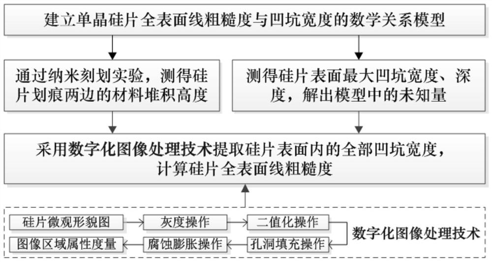
[0045] see Figure 1 to Figure 6 , an image processing-based method for predicting the full surface line roughness of a single crystal silicon wafer cut by a wire saw, comprising the following steps:

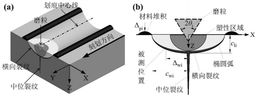
[0046] 1) Establish a mathematical relationship model between the full surface line roughness of a single crystal silicon wafer and the width of the pit. The pits are formed by removing the material above the lateral cracks of the single crystal silicon wafer.

[0047] The whole surface line roughness of the single crystal silicon wafer includes the roughness perpendicular to the crack and the roughness parallel to the crack direction.

[0048] The mathematical relationship model between the full surface line roughness of the single crystal silicon wafer and the width of the pit includes a roughness calculation model perpendicular to the crack and a roughness calculation model parallel to the crack direction.

[0049] The roughness calculation model perpendicular to the crack ...

Embodiment 2

[0075] A method for predicting the full surface line roughness of a single crystal silicon wafer cut by a wire saw based on image processing, the steps are as follows:

[0076] (1) Considering the scratch direction and material accumulation effect on the surface of the silicon wafer, a mathematical relationship model between the full surface line roughness of the single crystal silicon wafer and the width of the pit is established.

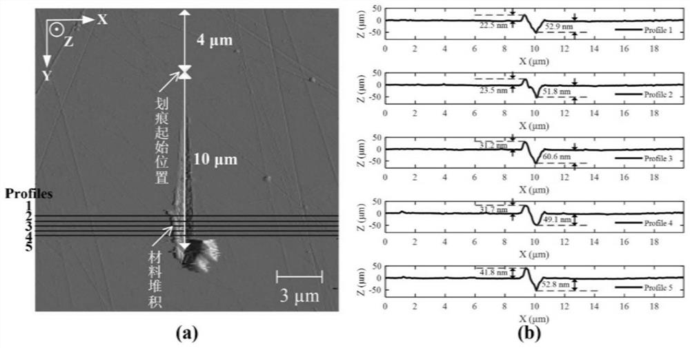
[0077] (2) Carry out nano-scribing experiments on the surface of silicon wafers, measure the material stacking heights on both sides of the scratches, and bring them into the mathematical relationship model between the overall surface line roughness and pit width of single-crystal silicon wafers.

[0078] (3) Obtain the microscopic surface morphology of the tested single crystal silicon wafer, measure the maximum pit width and depth, and solve the unknown quantity in the mathematical relationship model between the full surface line roughness of the...

Embodiment 3

[0099] An experiment based on image processing of wire saw cutting single crystal silicon wafer full surface line roughness prediction method, the content is as follows:

[0100] 1. Experiment object:

[0101] Take the single crystal silicon wafer processed by the diamond wire saw cutting machine (QPJ1665) produced by Dalian Liancheng CNC Machine Co., Ltd. as an example. The characteristics of the silicon wafer material are: density ρ=2.33 g / cm 3 , Young's modulus E=129.5GPa, Poisson's ratio ν=0.24, hardness H=11.0GPa, fracture toughness The size of the silicon wafer is: length×width×height=156×156×0.2mm. The sawing wire parameters are: sawing wire diameter D=86.9μm, sawing wire core diameter d=74.4μm, abrasive particle diameter d m =12μm, the height H of abrasive grains m =5.4μm, abrasive grain density N=424 / mm 2 . The process parameters are: wire feed speed v f =1.5mm / min, saw wire speed v s = 1800 m / min.

[0102] 2. Experimental process:

[0103] (1) Considering ...


PUM

PropertyMeasurementUnit
densityaaaaaaaaaa
hardnessaaaaaaaaaa
Poisson's ratioaaaaaaaaaa

Abstract

The invention discloses a method for predicting the whole-surface line roughness of a monocrystalline silicon wafer cut by a fretsaw based on image processing. The method comprises the following steps: 1) establishing a mathematical relationship model between the whole-surface line roughness of the monocrystalline silicon wafer and the width of a pit; the pit is formed by removing a material above a transverse crack of the monocrystalline silicon wafer; and 2) obtaining the microscopic surface topography of the monocrystalline silicon wafer, extracting the widths of all the pits of the monocrystalline silicon wafer, and inputting the widths of all the pits into the mathematical relationship model between the full-surface line roughness of the monocrystalline silicon wafer and the widths of the pits to obtain the full-surface line roughness of the monocrystalline silicon wafer. According to the method, the whole surface line roughness of the silicon wafer can be accurately predicted only by obtaining the microtopography of the monocrystalline silicon wafer in the same batch, and the manual measurement time is greatly shortened.

Description

technical field [0001] The invention relates to the technical field of machining and manufacturing, in particular to a method for predicting the line roughness of the entire surface of a single crystal silicon wafer cut by a wire saw based on image processing. Background technique [0002] Monocrystalline silicon is a typical brittle optical material with low thermal expansion coefficient, high temperature resistance, good radiation resistance, etc. It is widely used in large-scale integrated circuits and photovoltaic solar energy industries. The processing flow of a single crystal silicon wafer is generally single crystal pulling, outer circle grinding, cutting, chamfering, grinding, etching, cleaning and polishing. The cutting methods mainly include free abrasive wire saw cutting and fixed abrasive wire saw cutting. Free abrasive wire saw cutting has disadvantages such as low cutting efficiency, slow wire running speed, short service life of saw wire, difficulty in slurry...

Claims


Application Information

Patent Timeline
Patent Type & Authority Applications(China)
IPC IPC(8): G06F30/20G06F30/10G06Q10/04G06F111/14
CPCG06F30/20G06F30/10G06Q10/04G06F2111/14
Inventor 尹莘新肖华攀
Owner CHONGQING UNIV
Why Eureka
Try Eureka