High-speed modulation high-power fundamental mode semiconductor laser chip and use method thereof

A high-power laser technology, applied in the structure of semiconductor lasers, lasers, and optical waveguide semiconductors, can solve problems such as low heat dissipation efficiency, adverse effects on device reliability, and device failure.

Pending Publication Date: 2022-05-31
Shandong Huaguang Optoelectronics Co. Ltd.
View PDF1 Cites 0 Cited by
  • Summary
  • Abstract
  • Description
  • Claims
  • Application Information

AI Technical Summary

Problems solved by technology

However, the inventors found that in practical applications, the P-side metal of this inverted structure is very prone to fracture, resulting in device failure. At the same time, due to the inverted structure, the lower cavity will cause a change in local refractive index and low heat dissipation efficiency. problems that adversely affect the reliability of the device
In addition, this patented technology still cannot solve the problem of electro-optical delay and improve frequency chirp

Method used


Image

  • High-speed modulation high-power fundamental mode semiconductor laser chip and use method thereof
  • High-speed modulation high-power fundamental mode semiconductor laser chip and use method thereof
  • High-speed modulation high-power fundamental mode semiconductor laser chip and use method thereof

Examples


Embodiment Construction

[0026] It should be noted that the following detailed description is exemplary and intended to provide further explanation of the present invention. Unless defined otherwise, all technical and scientific terms used herein have the same meaning as commonly understood by one of ordinary skill in the art to which this invention belongs.

[0027] It should be noted that the terminology used here is only for describing specific embodiments, and is not intended to limit exemplary embodiments according to the present invention. As used herein, singular forms are intended to include plural forms unless the context clearly dictates otherwise. In addition, it should also be understood that when the terms "comprising" and / or "comprises" are used in this specification, it indicates the presence of features, steps, operations, means, components and / or their combination.

[0028] For the convenience of description, if the words "up", "down", "left" and "right" appear in the present inventi...


PUM

PropertyMeasurementUnit
Depthaaaaaaaaaa

Abstract

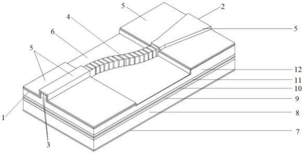
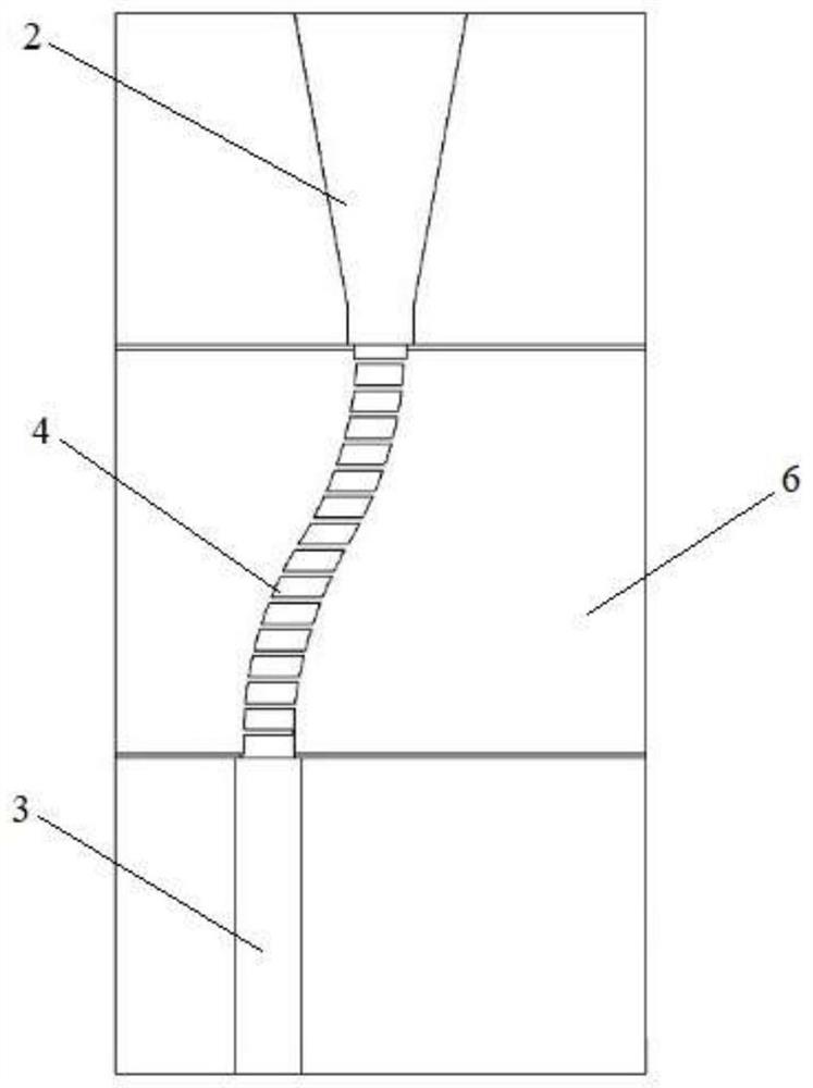
The invention discloses a high-speed modulation high-power fundamental mode semiconductor laser chip which comprises an active conical waveguide, a passive bent waveguide and an active oscillation stage waveguide which are arranged on a chip insulating layer. Wherein the active conical waveguide and the active oscillation stage waveguide are connected through the passive bent waveguide, and the passive bent waveguide is connected with the narrow end of the active conical waveguide. Meanwhile, the active conical waveguide and the active oscillation stage waveguide are both provided with electrodes, and the passive bent waveguide is not provided with an electrode, so that the active conical waveguide and the active oscillation stage waveguide are insulated and isolated. A new current injection structure is redesigned, namely, an active oscillation stage waveguide for generating high-quality fundamental transverse mode seed light, a passive bent waveguide for realizing high-order mode filtering and line width compression, and an active conical waveguide for realizing fundamental mode light one-way amplification. The electro-optical delay of each chip and the frequency chirp effect caused by the change of carrier concentration are effectively improved.

Description

technical field [0001] The invention relates to the technical field of semiconductor lasers, in particular to a high-speed modulated high-power fundamental-mode semiconductor laser chip and a method for using the same. Background technique [0002] The information disclosed in the Background of the Invention is only intended to increase the understanding of the general background of the invention, and is not necessarily to be taken as an acknowledgment or any form of suggestion that the information constitutes the prior art that is already known to those skilled in the art. [0003] High-power semiconductor lasers are widely used in pumping, optical communication, medical treatment, laser detection and other fields, and the performance requirements of semiconductor lasers are also getting higher and higher. Laser modulation refers to the process of using laser as a carrier to carry a low-frequency telecommunication system. Laser modulation is divided into internal modulation...

Claims


Application Information

Patent Timeline
IPC IPC(8): H01S5/10H01S5/22
CPCH01S5/1014H01S5/101H01S5/2222
Inventor 孙春明吴凯苏建刘琦朱振
Owner Shandong Huaguang Optoelectronics Co. Ltd.
Why Eureka
Try Eureka