A kind of ridge waveguide semiconductor laser and its preparation method

A ridge waveguide and semiconductor technology is applied in the field of ridge waveguide semiconductor lasers and their preparation, which can solve the problems of low laser output power and low laser slope efficiency, improve photoelectric conversion efficiency and slope efficiency, and realize high-power fundamental mode. The effect of laser lasing

Active Publication Date: 2021-02-23
SUZHOU INST OF NANO TECH & NANO BIONICS CHINESE ACEDEMY OF SCI +1
View PDF8 Cites 0 Cited by
  • Summary
  • Abstract
  • Description
  • Claims
  • Application Information

AI Technical Summary

Problems solved by technology

In the common ridge waveguide semiconductor lasers commonly used at present, the stripe width is generally 1.5-3 μm, and the thickness of the upper confinement layer is about 0.1 μm. The expansion of the laser caused the slope efficiency of the laser working in the fundamental mode to be lower than the slope efficiency of the laser working in the multimode, and because of its small strip width, the output power of the laser will be significantly lower, making the application of this ridge waveguide Gallium nitride-based lasers with the structure are difficult to be widely used in various fields that require high output power or slope efficiency of the laser

Method used


Image

  • A kind of ridge waveguide semiconductor laser and its preparation method
  • A kind of ridge waveguide semiconductor laser and its preparation method
  • A kind of ridge waveguide semiconductor laser and its preparation method

Examples


Embodiment Construction

[0018] In order to make the object, technical solution and advantages of the present invention clearer, the specific implementation manners of the present invention will be described in detail below in conjunction with the accompanying drawings. Examples of these preferred embodiments are illustrated in the accompanying drawings. The embodiments of the invention shown in and described with reference to the drawings are merely exemplary, and the invention is not limited to these embodiments.

[0019] Here, it should also be noted that, in order to avoid obscuring the present invention due to unnecessary details, only the structures and / or processing steps that are closely related to the solution according to the present invention are shown in the drawings, and the relationship between them is omitted. Little other details.

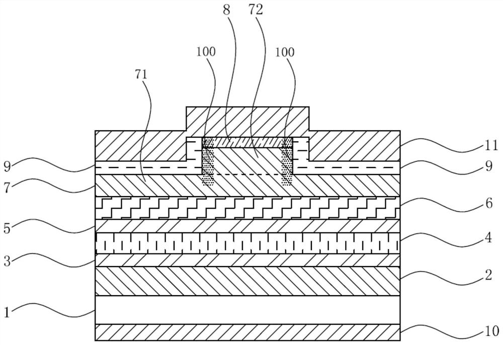
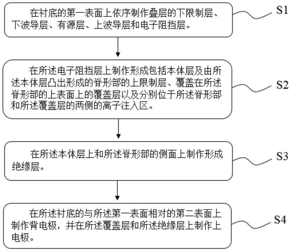
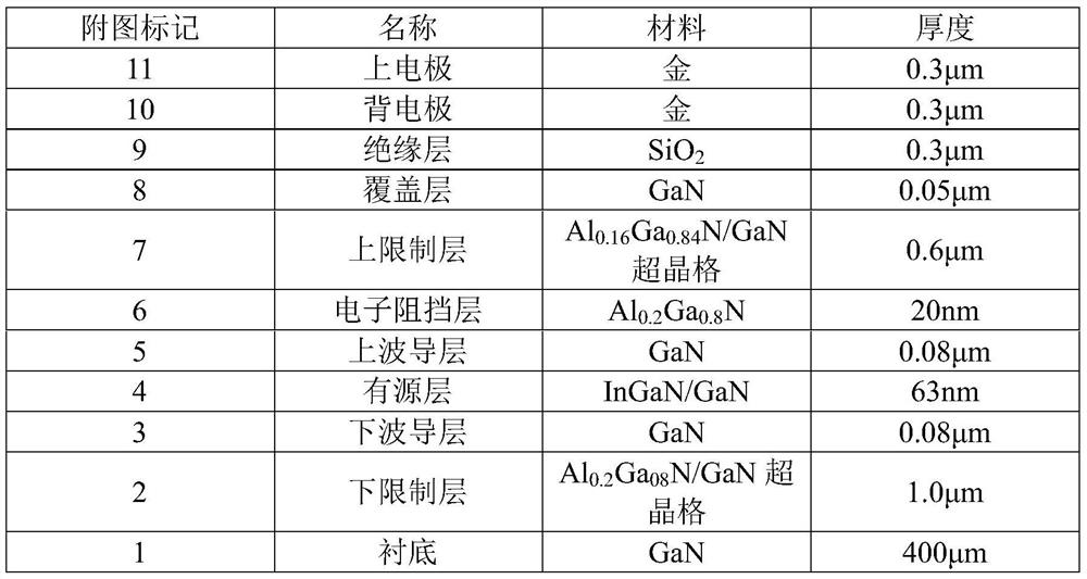
[0020] refer to figure 1 , the present embodiment provides a ridge waveguide semiconductor laser, comprising a substrate 1, a lower confinement layer 2, ...


PUM

PropertyMeasurementUnit
thicknessaaaaaaaaaa
thicknessaaaaaaaaaa
wavelengthaaaaaaaaaa

Abstract

The invention discloses a ridge-shaped waveguide semiconductor laser and a preparation method thereof. In the ridge-shaped waveguide semiconductor laser, ion implantation is performed on both sides of a ridge-shaped portion and both sides of a covering layer on the ridge-shaped portion, The ion implantation region is formed, and the carriers can almost only pass through the central region outside the ion implantation region. The difference between the gain of the fundamental mode and the high-order mode is used to suppress the lasing of the high-order mode, so that the ridge waveguide semiconductor laser can be The larger ridge stripe width can still work stably in the fundamental mode. Since carriers are only injected through the central region with high laser photon density, the photoelectric conversion efficiency and slope efficiency of the ridge waveguide semiconductor laser can be greatly improved. High power fundamental mode laser lasing.

Description

technical field [0001] The invention relates to the technical field of semiconductor lasers, in particular to a ridge waveguide semiconductor laser and a preparation method thereof. Background technique [0002] In the field of semiconductor lasers, due to the light confinement and current confinement in the direction parallel to the junction, the ridge waveguide structure is widely used in various semiconductor lasers. For example, in order to obtain a gallium nitride-based laser that works stably in the fundamental mode, a ridge waveguide structure with a small etching depth and a narrow strip width is usually used. In the common ridge waveguide semiconductor lasers commonly used at present, the stripe width is generally 1.5-3 μm, and the thickness of the upper confinement layer is about 0.1 μm. The expansion of the laser caused the slope efficiency of the laser working in the fundamental mode to be lower than the slope efficiency of the laser working in the multimode, an...

Claims


Application Information

Patent Timeline
Patent Type & Authority Patents(China)
IPC IPC(8): H01S5/22H01S5/32
CPCH01S5/22H01S5/32
Inventor 胡俊杰李德尧张立群刘建平张书明杨辉
Owner SUZHOU INST OF NANO TECH & NANO BIONICS CHINESE ACEDEMY OF SCI
Why Eureka
Try Eureka