A kind of high-power semiconductor chip and its preparation method

一种半导体、高功率的技术,应用在半导体激光器、光波导半导体的结构、激光器零部件等方向,能够解决远场多峰等问题,达到消除远场双峰、抑制侧向光强度周期震荡、抑制激射的效果

Active Publication Date: 2020-06-02
EVERBRIGHT INST OF SEMICON PHOTONICS CO LTD +1
View PDF5 Cites 0 Cited by
  • Summary
  • Abstract
  • Description
  • Claims
  • Application Information

AI Technical Summary

Problems solved by technology

[0003] In view of this, an embodiment of the present invention provides a high-power semiconductor chip and its preparation method to solve the problem of far-field multi-peaks caused when controlling and suppressing high-order optical lateral mode lasing

Method used


Image

  • A kind of high-power semiconductor chip and its preparation method
  • A kind of high-power semiconductor chip and its preparation method

Examples


Embodiment Construction

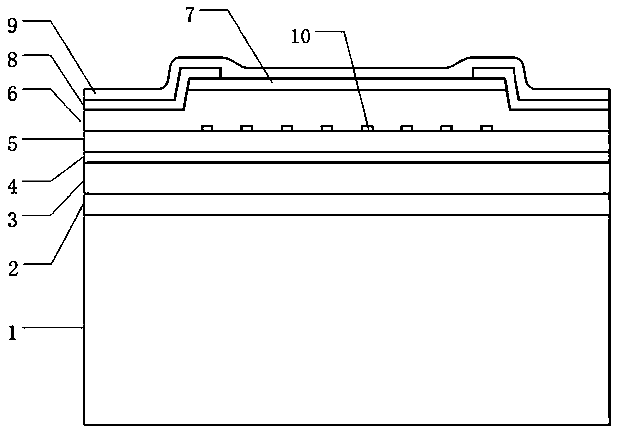
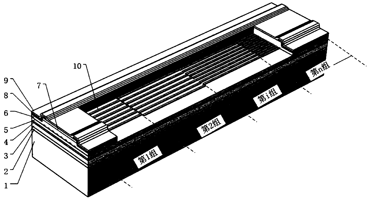
[0018] In order to make the purpose, technical solutions and advantages of the embodiments of the present invention clearer, the technical solutions in the embodiments of the present invention will be clearly and completely described below in conjunction with the drawings in the embodiments of the present invention. Obviously, the described embodiments It is a part of embodiments of the present invention, but not all embodiments. Based on the embodiments of the present invention, all other embodiments obtained by those skilled in the art without creative efforts shall fall within the protection scope of the present invention.

[0019] This invention may be embodied in many different forms and should not be construed as limited to the embodiments set forth herein. Rather, these embodiments are provided so that this disclosure will be thorough and complete and will fully convey the concept of the invention to those skilled in the art, and the present invention will only be defin...


PUM

PropertyMeasurementUnit
poweraaaaaaaaaa

Abstract

The invention discloses a high-power semiconductor chip and a preparation method thereof. The semiconductor chip comprises: a substrate, a lower confinement layer, a lower waveguide layer, an active layer, an upper waveguide layer, a lateral grating layer, and a substrate arranged sequentially from bottom to top. An upper confinement layer, a contact layer, a current isolation medium layer, and a metal layer; wherein, the lateral grating layer includes multiple groups of lateral gratings, and the multiple groups of lateral gratings are arranged in sequence along the first direction, and the periods of the multiple groups of lateral gratings are different , each group of side gratings includes a plurality of gratings, the plurality of gratings are arranged along the second direction, and the first direction intersects the second direction. By setting the lateral grating layer in the waveguide, the propagation loss of the high-order light lateral mode in the waveguide is improved, and the purpose of suppressing the lasing of the high-order light lateral mode is achieved; multiple groups of gratings with different periods are set to suppress the gain modulation caused by a single grating. And the lasing of the intensity oscillation light mode caused by the modulation of the refractive index can suppress the periodic oscillation of the lateral light intensity and eliminate the double peaks in the far field.

Description

technical field [0001] The invention relates to the field of semiconductor optoelectronics, in particular to a high-power semiconductor chip and a preparation method thereof. Background technique [0002] The development direction of high-power semiconductor laser chips is higher output optical power and higher brightness. Increasing the width of the light-emitting area of ​​the laser chip and preparing a semiconductor laser chip with a wide waveguide is an effective means to increase the optical power. For example, the power of a semiconductor laser chip with a waveguide width of about 100-200 microns can reach more than 10W. However, a problem caused by the increase in the width of the light-emitting region is that when the chip is working, dozens or even more high-order light modes are simultaneously lased laterally, resulting in an increase in the divergence angle. The currently used method to suppress high-order light lateral mode lasing is to introduce multiple grati...

Claims


Application Information

Patent Timeline
Patent Type & Authority Patents(China)
IPC IPC(8): H01S5/12
CPCH01S5/1237H01S5/1231H01S5/22H01S5/1225H01S2301/166H01S5/0287H01S5/2027H01S5/1215
Inventor 谭少阳王俊徐红闵大勇
Owner EVERBRIGHT INST OF SEMICON PHOTONICS CO LTD
Why Eureka
Try Eureka