High-power LED and preparation method thereof
A high-power, growth-rate technology, applied in semiconductor devices, electrical components, circuits, etc., can solve the problems of imperfect design of LED quantum wells and electron blocking layers, uneven distribution of carriers, and low hole injection efficiency. Achieve the effect of realizing large-scale production applications, reducing the strength of the polarization electric field, and increasing the effective barrier height
- Summary
- Abstract
- Description
- Claims
- Application Information
AI Technical Summary
Problems solved by technology
Method used
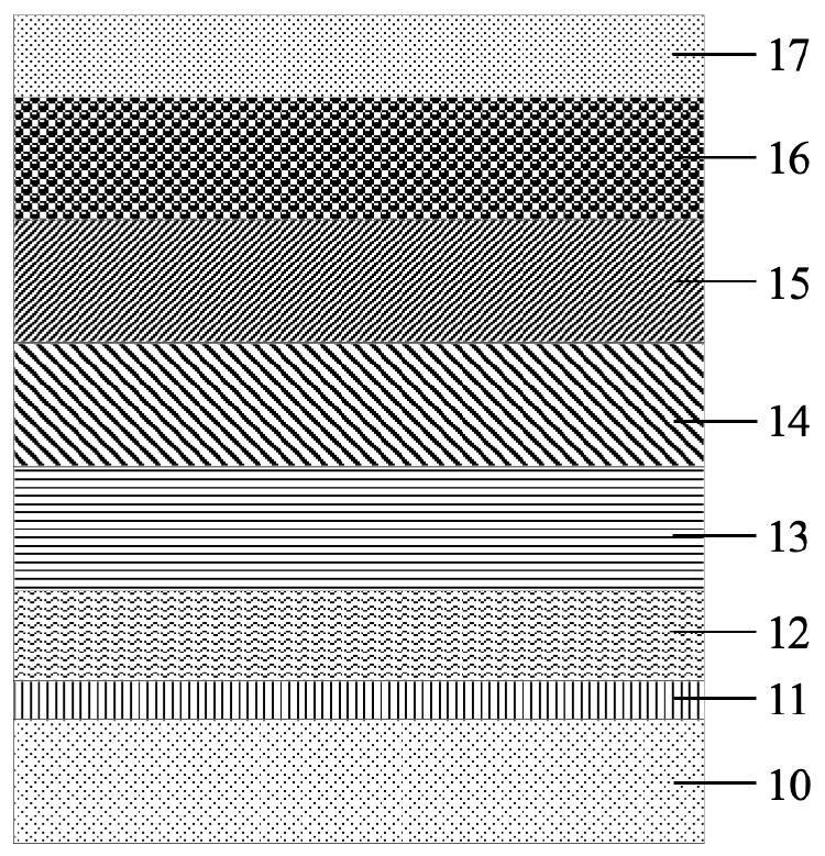
Image

Examples
Embodiment 1
[0024] In the above S1, the AlN buffer layer was grown by physical vapor deposition method, the growth temperature was 400° C., and the thickness of the AlN buffer layer was found to be 5 nm.
[0025] In the above S2, the InGaN buffer layer was grown on the inventive AlN buffer layer by metal-organic chemical vapor deposition, the reaction chamber pressure was 50 torr, the growth temperature was 1000°C, the beam current ratio V / III was 3000, and the growth rate was 2 μm / h.
[0026] In the above S3, the non-doped InGaN layer was grown on the inventive InGaN buffer layer by metal-organic chemical vapor deposition. The rate is 2 μm / h.
[0027] In the above S4, the n-type doped InGaN layer is grown on the non-doped InGaN layer by metal-organic chemical vapor deposition method. The process conditions are: the reaction chamber pressure is 50 torr, the growth temperature is 1000 °C, and the beam current ratio V / III is 3000, the growth rate is 2μm / h; the invention n-type doped InGaN ...
Embodiment 2
[0032] In the above S1, the AlN buffer layer was grown by physical vapor deposition method, the growth temperature was 450° C., and the thickness of the AlN buffer layer was found to be 27 nm.
[0033] In the above S2, the InGaN buffer layer was grown on the inventive AlN buffer layer by metal-organic chemical vapor deposition, the reaction chamber pressure was 175torr, the growth temperature was 1130°C, the beam current ratio V / III was 4000, and the growth rate was 3μm / h.
[0034] In the above S3, the non-doped InGaN layer was grown on the inventive InGaN buffer layer by metal-organic chemical vapor deposition. The rate is 3 μm / h.
[0035] In the above S4, the n-type doped InGaN layer was grown on the non-doped InGaN layer by the metal organic chemical vapor deposition method. The process conditions were: the reaction chamber pressure was 175torr, the growth temperature was 1130°C, and the beam current ratio V / III was 4000, the growth rate is 3μm / h; the invention n-type dope...
Embodiment 3
[0040] In the above S1, the AlN buffer layer was grown by physical vapor deposition method, the growth temperature was 500° C., and the thickness of the AlN buffer layer was found to be 50 nm.
[0041] In the above S2, the InGaN buffer layer was grown on the inventive AlN buffer layer by metal-organic chemical vapor deposition, the reaction chamber pressure was 300 torr, the growth temperature was 1260°C, the beam current ratio V / III was 5000, and the growth rate was 4 μm / h.
[0042] In the above S3, the non-doped InGaN layer was grown on the inventive InGaN buffer layer by metal-organic chemical vapor deposition. The rate is 4 μm / h.
[0043] In the above S4, the n-type doped InGaN layer is grown on the non-doped InGaN layer by the metal organic chemical vapor deposition method. The process conditions are: the reaction chamber pressure is 300torr, the growth temperature is 1260°C, and the beam current ratio V / III is 5000, the growth rate is 4μm / h; the n-type doped InGaN layer...
PUM
| Property | Measurement | Unit |
|---|---|---|
| thickness | aaaaa | aaaaa |
| thickness | aaaaa | aaaaa |
| thickness | aaaaa | aaaaa |
Abstract
Description
Claims
Application Information
 - Generate Ideas
- Intellectual Property
- Life Sciences
- Materials
- Tech Scout
- Unparalleled Data Quality
- Higher Quality Content
- 60% Fewer Hallucinations
Browse by: Latest US Patents, China's latest patents, Technical Efficacy Thesaurus, Application Domain, Technology Topic, Popular Technical Reports.
© 2025 PatSnap. All rights reserved.Legal|Privacy policy|Modern Slavery Act Transparency Statement|Sitemap|About US| Contact US: help@patsnap.com