Liquid crystal writing device voltage control system and method for realizing local erasing
A technology for a voltage control system and a writing device, which is applied in nonlinear optics, static indicators, optics, etc., can solve the problems of occupying space, complex circuit structure, and many circuit components, so as to reduce production costs, simplify circuit structure, Good user experience
- Summary
- Abstract
- Description
- Claims
- Application Information
AI Technical Summary
Problems solved by technology
Method used
Image
Examples
Embodiment 1
[0031] In one or more embodiments, a liquid crystal writing device voltage control system for realizing partial erasing is disclosed.
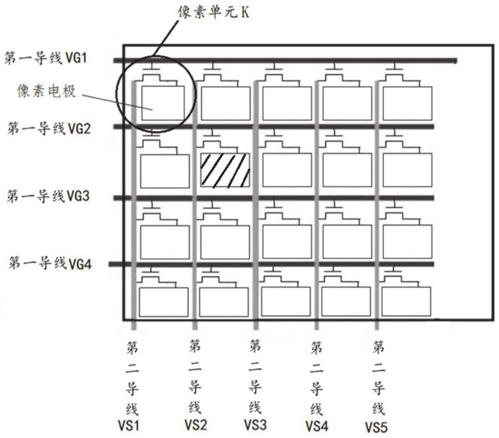
[0032] Wherein, the liquid crystal writing device includes: a conductive layer, a bistable liquid crystal layer and a base layer arranged in sequence; the conductive layer is not divided; refer to figure 1 A number of pixel units arranged in an array are integrated on the base layer, and each pixel unit is provided with a pixel electrode and a TFT connected to the pixel electrode; a number of first wires that are supplied with a control voltage for turning on or off the TFT; a plurality of second wires supplying the TFT input voltage;
[0033] refer to figure 1 , the first wire is shared by the pixel units in the same row, and the second wire is shared by the pixel units in the same column. In this embodiment, corresponding to each vertical column and each horizontal row of the pixel unit, a plurality of first wires and a plurality of second...
Embodiment 2
[0055] In one or more embodiments, a liquid crystal writing device voltage control method for realizing partial erasing is disclosed, including:
[0056] Connecting the first wires on the base layer of the liquid crystal writing device to different output terminals of the first VFD drive chipset;
[0057] Connecting each second wire on the base layer of the liquid crystal writing device to different output terminals of the second VFD driving chipset;
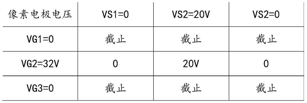
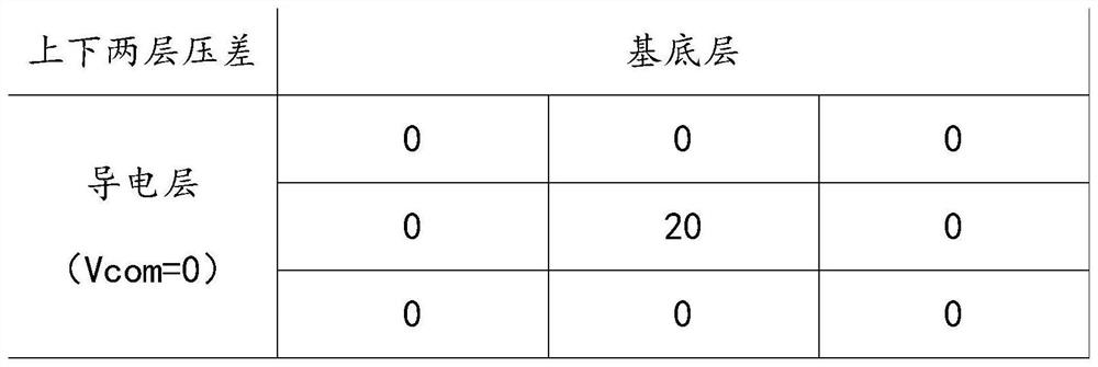
[0058] Apply a set voltage to the conductive layer, and control the output voltages of the output terminals of the first VFD driver chip set and the second VFD driver chip set through the main controller, so that the pixel unit covering the partial erasing area on the base layer and the conductive layer The electric field between them reaches the erasing electric field, which can realize partial erasing; while the electric field formed in other regions cannot realize erasing.
[0059] It should be noted that the specific implem...
Embodiment 3
[0061] In one or more embodiments, a liquid crystal writing device with partial erasing function is disclosed, including a conductive layer, a bistable liquid crystal layer and a base layer arranged in sequence; the conductive layer is not divided; an array is integrated on the base layer A number of pixel units arranged in a shape, each pixel unit is provided with a pixel electrode and a TFT connected to the pixel electrode; a number of first wires that are supplied with a control voltage for turning on or off the TFT; a number of first wires that are supplied with an input voltage for the TFT two wires;
[0062] The first wire is shared by the pixel units in the same row, and the second wire is shared by the pixel units in the same column. In this embodiment, corresponding to each vertical column and each horizontal row of the pixel unit, a plurality of first wires and a plurality of second wires are respectively integrated; the layout directions of the first wires and the s...
PUM
 Abstract
Description
Claims
Application Information
 - R&D Engineer
- R&D Manager
- IP Professional
- Industry Leading Data Capabilities
- Powerful AI technology
- Patent DNA Extraction
Browse by: Latest US Patents, China's latest patents, Technical Efficacy Thesaurus, Application Domain, Technology Topic, Popular Technical Reports.
© 2024 PatSnap. All rights reserved.Legal|Privacy policy|Modern Slavery Act Transparency Statement|Sitemap|About US| Contact US: help@patsnap.com


