Method for testing high-resistance failure of semiconductor device

A test method and semiconductor technology, applied in the direction of single semiconductor device testing, instruments, measuring devices, etc., can solve the problems of no input terminal and output terminal test resistance, complex interconnection line interaction, etc.

Pending Publication Date: 2022-04-15
SHANGHAI HUALI MICROELECTRONICS CORP
View PDF0 Cites 0 Cited by
  • Summary
  • Abstract
  • Description
  • Claims
  • Application Information

AI Technical Summary

Problems solved by technology

However, due to the complex interaction of interconnection lines in different regions in semiconductor devices, there are no fixed input terminals and output terminals for testing resistance

Method used


Image

  • Method for testing high-resistance failure of semiconductor device
  • Method for testing high-resistance failure of semiconductor device
  • Method for testing high-resistance failure of semiconductor device

Examples


Embodiment Construction

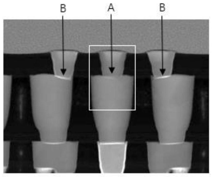
[0029] The specific implementation manner of the present invention will be described in more detail below with reference to schematic diagrams. The advantages and features of the present invention will be more apparent from the following description. It should be noted that all the drawings are in a very simplified form and use imprecise scales, and are only used to facilitate and clearly assist the purpose of illustrating the embodiments of the present invention.

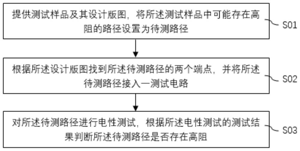
[0030] figure 2 It is a flowchart of a testing method for high-resistance failure of a semiconductor device provided by an embodiment of the present invention.

[0031] refer to figure 2 , the test method for high-resistance failure of the semiconductor device provided in this embodiment includes:

[0032] Step S01: Provide a test sample and its design layout, and set a path that may have high resistance in the test sample as the path to be tested;

[0033] Step S02: Find two endpoints of the path to be teste...


PUM


Abstract

The invention provides a semiconductor device high-resistance failure test method, which comprises the following steps: providing a test sample and a design layout thereof, and setting a path in which high resistance possibly exists in the test sample as a to-be-tested path; finding out two end points of the to-be-tested path according to the design layout, and connecting the to-be-tested path to a test circuit; and performing an electrical test on the to-be-tested path, and judging whether the to-be-tested path has high resistance or not according to a test result of the electrical test. By setting the to-be-tested path of the semiconductor device and performing the electrical test on the to-be-tested path, whether the high-resistance failure exists in the to-be-tested path or not is accurately judged, and the test efficiency is improved.

Description

technical field [0001] The invention relates to the technical field of semiconductor testing, in particular to a testing method for high-resistance failure of semiconductor devices. Background technique [0002] The semiconductor manufacturing process is divided into the front-end device process and the back-end metal interconnection process. The role of the back-end metal interconnection layer is to lead out the front-end devices for testing or work. In the semiconductor manufacturing process, due to the limitation of design level and process technology, the interconnection lines in semiconductor devices often suffer from short-circuit failure or open-circuit failure. However, the failure of some semiconductor devices is caused by the high-resistance contact of the interconnection line. For the failure caused by high resistance rather than short circuit, common analysis methods (such as VC positioning technology) cannot effectively locate the failure location. [0003] To ...

Claims


Application Information

Patent Timeline
IPC IPC(8): G01R31/26G01R27/02
Inventor 段淑卿武城高金德
Owner SHANGHAI HUALI MICROELECTRONICS CORP
Why Eureka
Try Eureka