Supercharge Your Innovation With Domain-Expert AI Agents!

OLED display panel and preparation method thereof

A display panel and auxiliary layer technology, which is applied to electrical components, electrical solid devices, circuits, etc., can solve problems such as small black spots, vanishing spots, and short circuits of organic particles, so as to avoid short circuits and reduce the probability of dark spots and vanishing spots , The effect of reducing the risk of organic particles

Pending Publication Date: 2022-04-12
SHENZHEN CHINA STAR OPTOELECTRONICS SEMICON DISPLAY TECH CO LTD
View PDF0 Cites 0 Cited by
  • Summary
  • Abstract
  • Description
  • Claims
  • Application Information

AI Technical Summary

Problems solved by technology

[0005] Based on the existing technical problems, the present application provides an OLED display panel and its preparation method, which can solve the problem that the pixel definition layer in the prior art is the ink drop of hydrophobic material solution falling onto the anode, and the remaining Organic particles will cause a short circuit between the cathode and the anode on the surface, initially appearing as small black spots, and later will form a technical problem of vanishing points

Method used


Image

  • OLED display panel and preparation method thereof
  • OLED display panel and preparation method thereof
  • OLED display panel and preparation method thereof

Examples


Embodiment Construction

[0024] The following descriptions of the various embodiments refer to the accompanying drawings to illustrate specific embodiments in which the invention may be practiced. The directional terms mentioned in the present invention, such as [top], [bottom], [front], [back], [left], [right], [inside], [outside], [side], etc., are only for reference The orientation of the attached schema. Therefore, the directional terms used are used to illustrate and understand the present invention, but not to limit the present invention. In the figure, units with similar structures are indicated by the same reference numerals, and the dotted lines in the figure indicate that they do not exist in the structure, and only illustrate the shape and position of the structure.

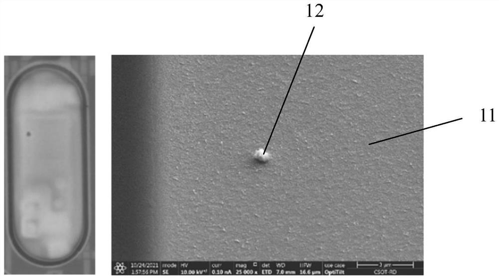
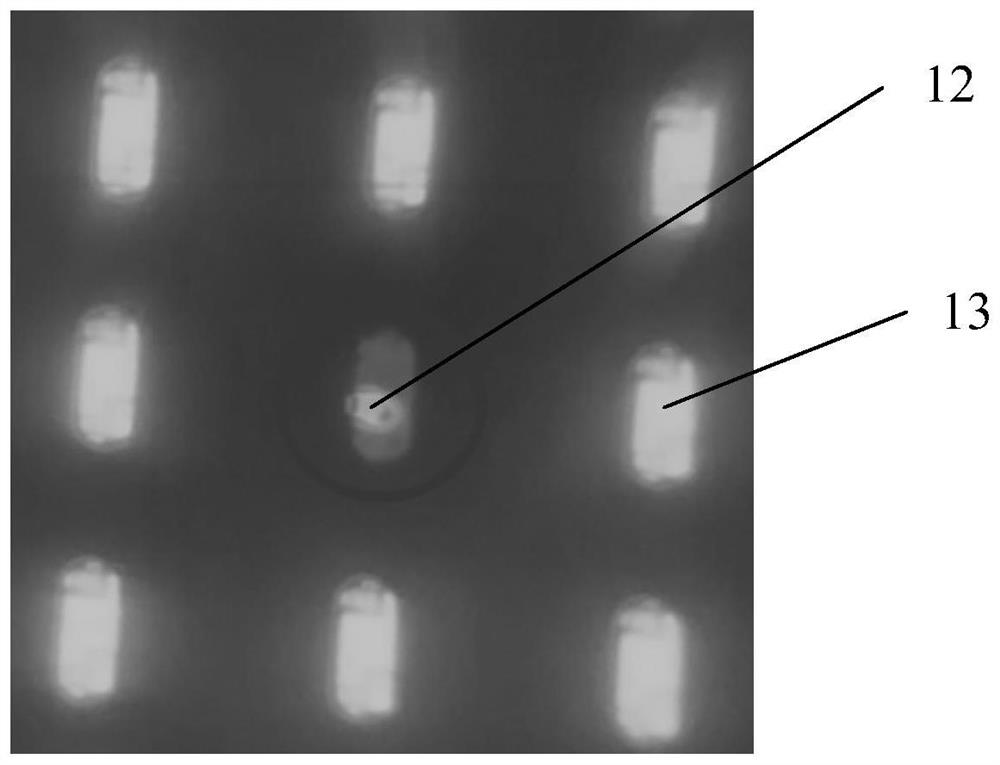
[0025] The present invention aims at the pixel definition layer in the OLED display panel preparation process in the prior art. The ink droplets of the hydrophobic material solution fall on the anode, and the residual organic...


PUM


Abstract

The invention provides a preparation method of an OLED display panel, and the method comprises the steps: S1, providing a substrate which comprises TFT devices arranged in an array, arranging anodes on the substrate in an array, and electrically connecting the anodes with the TFT devices; arranging an auxiliary layer on the anode; s2, forming a pixel definition layer on the substrate, wherein the anode and the auxiliary layer are arranged in a pixel opening of the pixel definition layer; s3, removing the auxiliary layer in the pixel opening and dust particles falling on the auxiliary layer by mistake, and then preparing a luminescent material layer and a cathode layer in the pixel opening; due to the fact that the risk that the organic matter particles on the surface of the anode are polluted in the manufacturing process is reduced, the risk that the cathode and the anode are short-circuited in the OLED device is avoided, the probability of dark spots and vanishing spots is reduced, and the display quality of the display panel is improved.

Description

technical field [0001] The invention relates to the field of display technology, in particular to an OLED display panel and a preparation method thereof. Background technique [0002] Organic Light Emitting Display (OLED) has self-illumination, low driving voltage, high luminous efficiency, short response time, high definition and contrast, nearly 180° viewing angle, wide operating temperature range, and can realize flexible display and With many advantages such as large-area full-color display, it is recognized by the industry as a display device with the most potential for development. [0003] An OLED display panel generally includes: a substrate, an anode disposed on the substrate, a hole injection layer disposed on the anode, a hole transport layer disposed on the hole injection layer, a light-emitting layer disposed on the hole transport layer, a device An electron transport layer on the light emitting layer, an electron injection layer on the electron transport layer...

Claims


Application Information

Patent Timeline
IPC IPC(8): H01L27/32
Inventor 黄旭覃事建
Owner SHENZHEN CHINA STAR OPTOELECTRONICS SEMICON DISPLAY TECH CO LTD
Features
  • R&D
  • Intellectual Property
  • Life Sciences
  • Materials
  • Tech Scout
  • Unparalleled Data Quality
  • Higher Quality Content
  • 60% Fewer Hallucinations
Learn More