Array substrate, preparation method thereof and display panel

A technology for array substrates and display areas, which is applied in semiconductor/solid-state device manufacturing, semiconductor devices, electrical components, etc., can solve problems such as increased manufacturing processes, and achieve the effect of reducing costs

Pending Publication Date: 2022-04-12
WUHAN CHINA STAR OPTOELECTRONICS SEMICON DISPLAY TECH CO LTD
View PDF0 Cites 0 Cited by
  • Summary
  • Abstract
  • Description
  • Claims
  • Application Information

AI Technical Summary

Problems solved by technology

[0003] Embodiments of the present invention provide an array substrate, its preparation method, and a display panel, so as to solve the technical problem of increasing the manufacturing process due to the addition of a patterned shielding layer under the channel of the active layer in the existing preparation method of the array substrate.

Method used


Image

  • Array substrate, preparation method thereof and display panel
  • Array substrate, preparation method thereof and display panel
  • Array substrate, preparation method thereof and display panel

Examples


Embodiment Construction

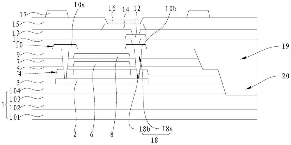
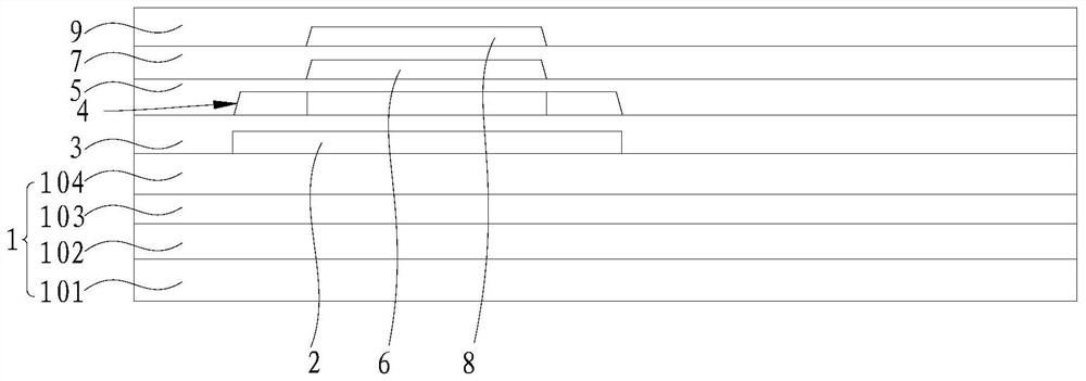
[0048] The following will clearly and completely describe the technical solutions in the embodiments of the present invention with reference to the accompanying drawings in the embodiments of the present invention. Obviously, the described embodiments are only some, not all, embodiments of the present invention. Based on the embodiments of the present invention, all other embodiments obtained by those skilled in the art without creative efforts fall within the protection scope of the present invention. In addition, it should be understood that the specific embodiments described here are only used to illustrate and explain the present invention, and are not intended to limit the present invention. In the present invention, unless stated to the contrary, the used orientation words such as "up" and "down" usually refer to up and down in the actual use or working state of the device, specifically the direction of the drawing in the drawings ; while "inside" and "outside" refer to ...


PUM

PropertyMeasurementUnit
thicknessaaaaaaaaaa
depthaaaaaaaaaa

Abstract

The invention discloses an array substrate and a preparation method thereof, and a display panel, the array substrate comprises a display area and a bending area, the display area comprises a substrate, a shielding layer, a barrier layer, an active layer and a first source-drain metal layer, the first source-drain metal layer is electrically connected with the active layer through a first sub-contact hole, and the first sub-contact hole is electrically connected with the active layer through a second sub-contact hole; the first source-drain metal layer is electrically connected with the shielding layer through the first sub-contact hole and the second sub-contact hole; the active layer and the shielding layer are used as the etching barrier layer, the contact hole and the first opening and the second opening located in the bending area are prepared through the same yellow light process, and compared with the prior art that the first opening and the second opening are prepared through one yellow light process, the yellow light process for preparing the second opening is omitted, and the production efficiency is improved. And the cost is reduced.

Description

technical field [0001] The present invention relates to the field of display technology, in particular to an array substrate, a preparation method thereof, and a display panel. Background technique [0002] OLED (Organic Light-Emitting Diode, Organic Light-Emitting Diode) technology has many advantages such as wide viewing angle, high contrast, fast response, low power consumption and foldable / flexible, usually adding a layer of patterned shielding under the active layer channel layer to shield the charge in the substrate (PI Charge), but this method will add a process to prepare the shielding layer, resulting in an increase in cost. Contents of the invention [0003] Embodiments of the present invention provide an array substrate, its preparation method, and a display panel, so as to solve the technical problem of increasing the manufacturing process due to the addition of a patterned shielding layer under the channel of the active layer in the existing preparation method...

Claims


Application Information

Patent Timeline
Patent Type & Authority Applications(China)
IPC IPC(8): H01L27/12H01L27/32H01L21/84
Inventor 白丹赵瑜
Owner WUHAN CHINA STAR OPTOELECTRONICS SEMICON DISPLAY TECH CO LTD
Why Eureka
Try Eureka