Silicon wafer processing fragmentation device and fragmentation method thereof

A technology of silicon wafers and mounts, applied in conveyor control devices, sorting, transportation and packaging, etc., can solve the problems of increased silicon wafer damage rate, affecting work efficiency, affecting use, etc., to reduce silicon wafer damage and improve Work efficiency and the effect of reducing production cost

Inactive Publication Date: 2022-04-12
朱秀洁
View PDF0 Cites 0 Cited by
  • Summary
  • Abstract
  • Description
  • Claims
  • Application Information

AI Technical Summary

Problems solved by technology

[0003] The piles of silicon wafers on the market need to be divided manually, which not only easily increases the damage rate of silicon wafers, but also affects work efficiency. Since the silicon wafers are piled together, the silicon wafers attract each other and it is difficult to divide them. And artificial slicing will also cause its surface to be scratched, affecting its use

Method used


Image

  • Silicon wafer processing fragmentation device and fragmentation method thereof
  • Silicon wafer processing fragmentation device and fragmentation method thereof
  • Silicon wafer processing fragmentation device and fragmentation method thereof

Examples


Embodiment Construction

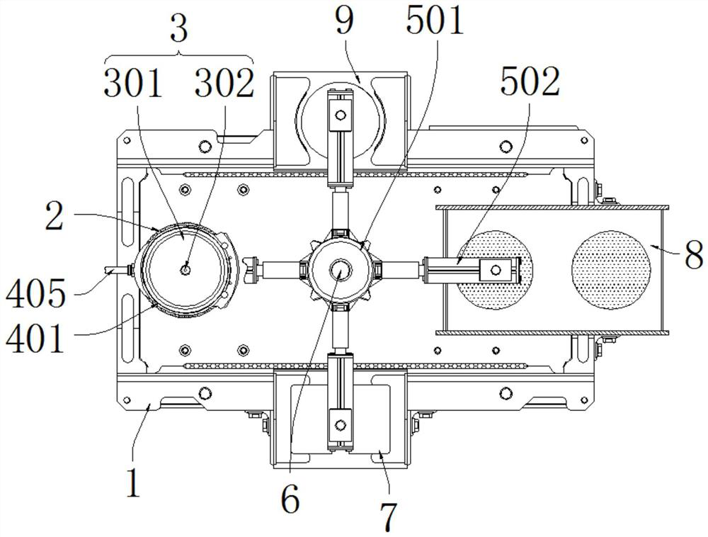
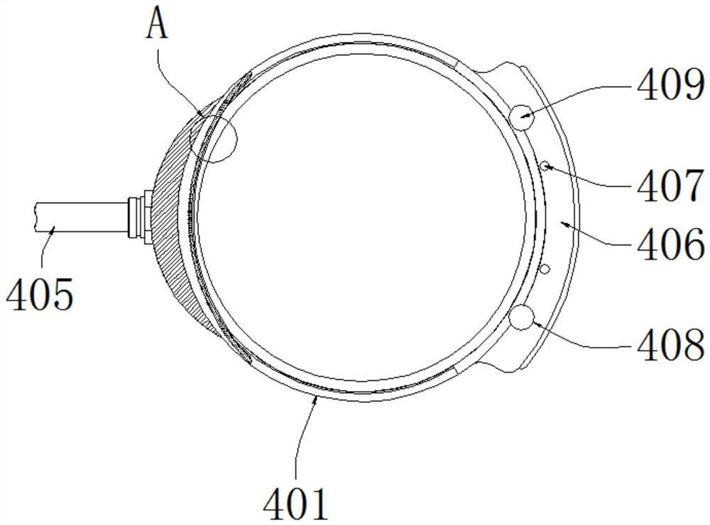
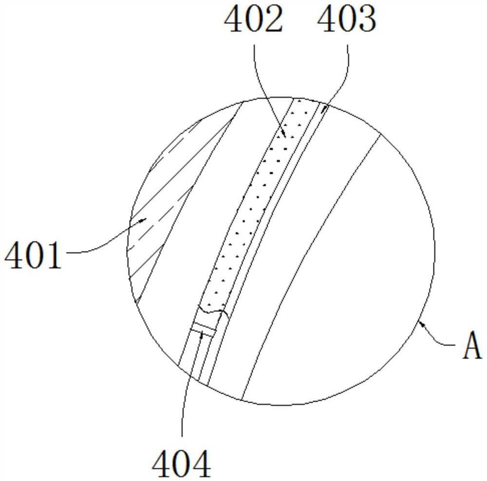
[0038] See Figure 1-7The present invention provides a technical solution: a silicon sheet processing fragmentation device and a fragmentation method thereof, including mounting seat 1 and auxiliary component 5, and a water tank 2 is mounted on the left side of the mount 1, and the water tank 2 is mounted inside. The frame 3, the carriage 3 is mounted, the bracket 3 includes an electric telescoping rod 301 and a dramable disk 302, and the electric telescoping rod 301 is connected to the trap 302, and the fragmentation mechanism 4 includes a set. The frame 401, the drive plate 402, the guide plate 403, the first nozzle 404, and the trachea 405, and the roller 402 is mounted on the left side of the ferrule 401, and the surface of the drive plate 402 is provided with a guide plate 403, and the guide plate 403 is inside. The first air nozzle 404 is mounted, and the air pipe 405 is connected to the right side of the first air nozzle 404, and the auxiliary component 5 is mounted to the m...


PUM


Abstract

The invention discloses a silicon wafer processing fragmentation device and a fragmentation method thereof, and relates to the technical field of silicon wafer processing, the silicon wafer processing fragmentation device comprises a mounting seat and an auxiliary assembly, a water tank is mounted on the left side of the mounting seat, a bearing frame is mounted in the water tank, a fragmentation mechanism is mounted outside the bearing frame, the bearing frame comprises an electric telescopic rod and an object dragging disc, and the object dragging disc is connected with the electric telescopic rod. The output end of the electric telescopic rod is connected with the object dragging disc. According to the wafer separating device, the multiple assemblies are arranged in a matched mode, automatic wafer separating of the silicon wafers can be achieved, excessive manual participation is not needed, the working efficiency can be improved, meanwhile, silicon wafer damage caused by misoperation can be reduced, wafer separating is completed in water, and the wafer separating efficiency is improved. By means of lubrication of the water liquid, the damage rate of the silicon wafers can be effectively reduced, the production cost of the silicon wafers can be reduced, the completeness degree of the surfaces of the silicon wafers can be automatically detected in the wafer separation process, the silicon wafers can be automatically classified and guided out, and the automation process of the silicon wafers is improved.

Description

Technical field [0001] The present invention relates to the field of silicon wafers, in particular a silicon-working fragmentation device and a fragmentation method thereof. Background technique [0002] During the production process, the silicon wafer needs to be cut, cleaned, and dried, but after the cut is completed, the silicon wafer is generally stacked together, and the silicon wafer needs to be divided into a piece of silicon carrier carrier. To the ultrasonic cleaning machine is cleaned. [0003] The stacks of silicon wafers in the market need to be artificially divided, which is not only likely to cause the wafer damage rate rising, while affecting the efficiency of work, which causes silicon wafers to attract each other, it is difficult to slide it. The artificial fragment also causes its surface to be scratched and affects its use. Inventive content [0004] It is an object of the present invention to provide a silicon-working fragmentation device and a fragmentation ...

Claims


Application Information

Patent Timeline
Patent Type & Authority Applications(China)
IPC IPC(8): B65G15/30B65G47/91B65G43/08B65G47/74B07C5/34B07C5/36
Inventor 朱秀洁
Owner 朱秀洁
Why Eureka
Try Eureka