Semiconductor device, method for manufacturing semiconductor device, and power conversion device
A technology of semiconductor and main conversion, applied in semiconductor/solid-state device manufacturing, output power conversion devices, semiconductor devices, etc., to achieve the effect of reducing the configuration area
- Summary
- Abstract
- Description
- Claims
- Application Information
AI Technical Summary
Problems solved by technology
Method used
Image

Examples
Embodiment approach 1
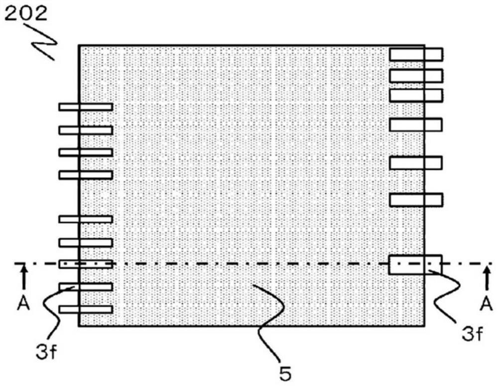
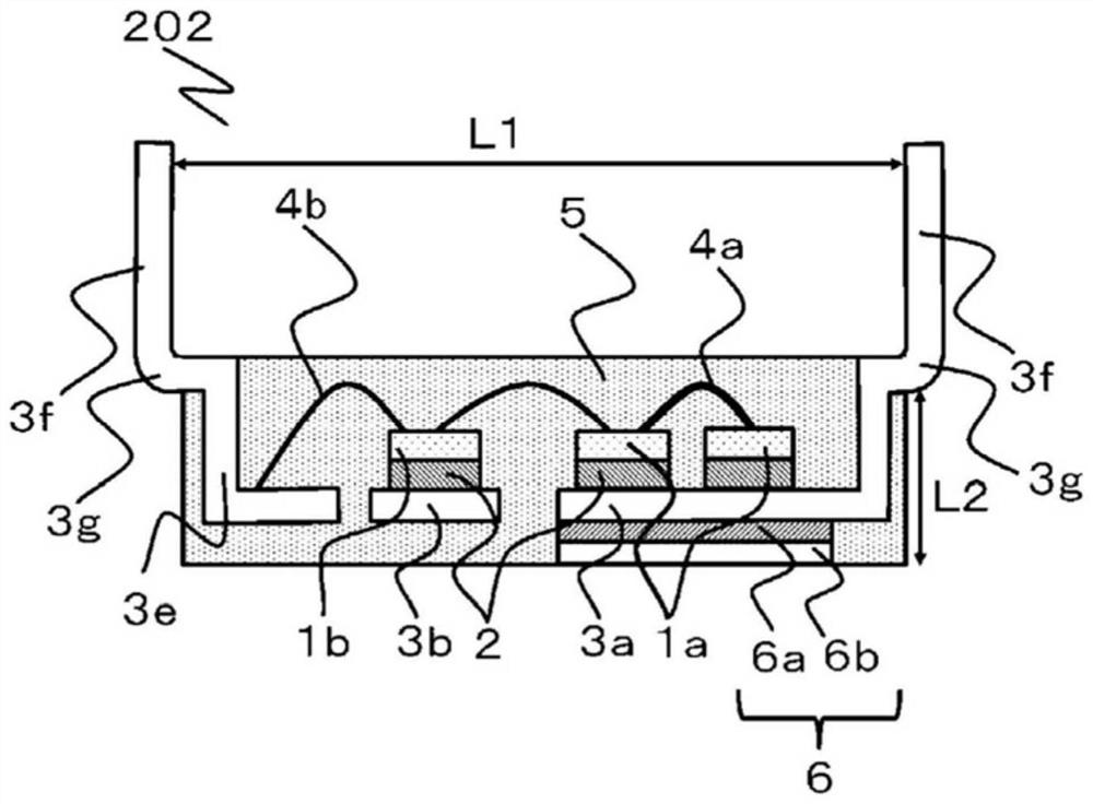
[0039] The structure of the semiconductor device according to Embodiment 1 will be described. figure 1 is a plan view showing the semiconductor device according to Embodiment 1, figure 2 yes figure 1 A cross-sectional view at line A-A in .
[0040] Such as figure 1 and figure 2 As shown, a semiconductor device 202 has a semiconductor element 1a, a semiconductor element 1b, a bonding material 2, an inner lead 3e, an outer lead 3f, a metal wire 4a, a metal wire 4b, a packaging resin 5, and an insulating heat dissipation plate 6. The inner lead 3e has a chip Pad 3a.
[0041] The semiconductor element 1a is a power semiconductor element. For example, IGBT (Insulated Gate Bipolar Transistor), MOSFET (Metal Oxide Semiconductor Field Effect Transistor), and FWD (Free Wheeling Diode) formed of silicon (Si). The length of one side of the semiconductor element 1 a is 3 mm to 13 mm in plan view.
[0042] The semiconductor element 1 a is mounted on the upper surface of the die...
Embodiment approach 2
[0121] Figure 17 is a plan view showing a semiconductor device 202c according to Embodiment 2, Figure 18 yes Figure 17 Sectional view at line E-E in . In addition, most configurations of the semiconductor device and the method of manufacturing the semiconductor device in this embodiment are the same as those of the first embodiment. Therefore, differences from the semiconductor device and the semiconductor device manufacturing method in Embodiment 1 will be described, and the same or corresponding structures will be given the same reference numerals, and their description will be omitted. The difference from Embodiment 1 lies in the following structure, that is, as Figure 17 ~ Figure 18 As shown, a second bent portion 3h is provided in addition to the first bent portion 3g to the outer lead 3f which is arranged in parallel to the exposed surface of the inner lead 3e exposed from the encapsulating resin 5 .
[0122] Such as Figure 17 and Figure 18 As shown, the inne...
Embodiment approach 3
[0133] Figure 21 It is a cross-sectional view showing a semiconductor device 202e according to the third embodiment. In addition, most configurations of the semiconductor device and the method of manufacturing the semiconductor device in this embodiment are the same as those of the first embodiment. Therefore, differences from the semiconductor device and the semiconductor device manufacturing method in Embodiment 1 will be described, and the same or corresponding structures will be given the same reference numerals, and their description will be omitted. The difference from Embodiment 1 lies in the following structure, that is, as Figure 21 As shown, a groove 9 is provided in the first bent portion 3g of the external lead 3f.
[0134] Figure 22 It is a top view showing the state after the component preparation process of preparing the lead frame 3 of the semiconductor device 202e. Such as Figure 22 As shown, a groove 9 having a depth of about 20% of the thickness of ...
PUM
| Property | Measurement | Unit |
|---|---|---|
| thickness | aaaaa | aaaaa |
| thickness | aaaaa | aaaaa |
| thermal conductivity | aaaaa | aaaaa |
Abstract
Description
Claims
Application Information
 - Generate Ideas
- Intellectual Property
- Life Sciences
- Materials
- Tech Scout
- Unparalleled Data Quality
- Higher Quality Content
- 60% Fewer Hallucinations
Browse by: Latest US Patents, China's latest patents, Technical Efficacy Thesaurus, Application Domain, Technology Topic, Popular Technical Reports.
© 2025 PatSnap. All rights reserved.Legal|Privacy policy|Modern Slavery Act Transparency Statement|Sitemap|About US| Contact US: help@patsnap.com