
An automatic processing device for semiconductor field effect transistors

A field effect transistor, automatic processing technology, applied in semiconductor/solid state device manufacturing, transportation and packaging, electrical components, etc., can solve the problems of inability to guarantee synchronization, large dynamic range, high input resistance, and reduce equipment costs. , Improve synchronization and ensure stability

Active Publication Date: 2022-08-09
先之科半导体科技(东莞)有限公司
View PDF3 Cites 0 Cited by
  • Summary
  • Abstract
  • Description
  • Claims
  • Application Information

AI Technical Summary

Problems solved by technology

[0002] Field Effect Transistor (FET) is a semiconductor device that controls the output loop current by controlling the electric field effect of the input loop. It is a voltage-controlled semiconductor device; it has the advantages of high input resistance (107~1015Ω), low noise, low power consumption, large dynamic range, easy integration, no secondary breakdown phenomenon, and wide safe working area. A strong competitor of polar transistors and power transistors, in the process of processing field effect transistors, heat sinks are generally installed on the casing of the transistors to ensure that the field effect transistors can operate stably when they are working. In technology, it is generally necessary to use the lifting device to drive the rotating device to process the heat sink, but the clamping equipment is also required to cooperate with the work during the processing, so as to match the rhythm of its work, but the installed device cannot be consistent with the movement of the lifting device Sex, synchronization cannot be guaranteed, and it is troublesome to adjust

Method used


Image

  • An automatic processing device for semiconductor field effect transistors
  • An automatic processing device for semiconductor field effect transistors
  • An automatic processing device for semiconductor field effect transistors

Examples


Embodiment Construction

[0041] In order to further understand the features, technical means, and specific goals and functions of the present invention, the present invention will be described in further detail below with reference to the accompanying drawings and specific embodiments.

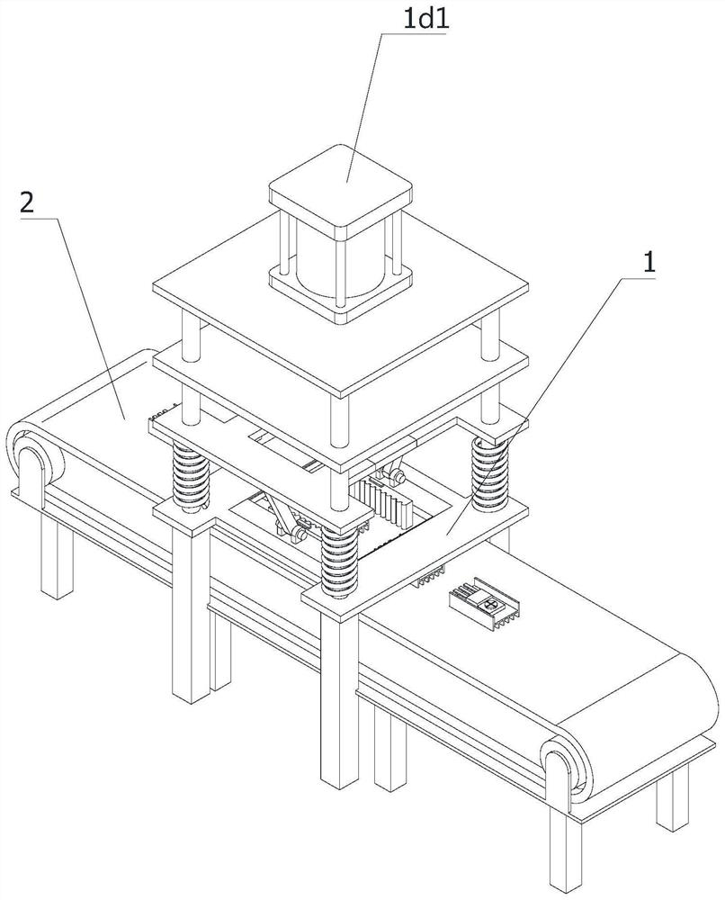
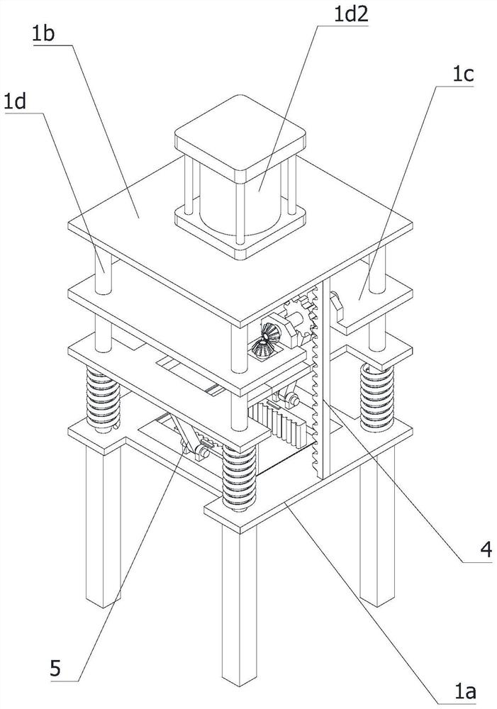
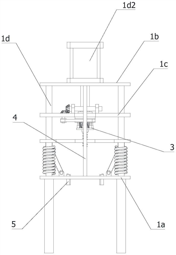
[0042] like Figure 1-12 shown:

[0043] An automatic processing device for semiconductor field effect transistors, comprising a frame 1 and a conveyor belt 2, the frame 1 spans the top of the conveyor belt 2, and the frame 1 is also provided with a support platform 1a, a top plate 1b, a transmission plate 1c, Linear driver 1d1 for driving transmission plate 1c, rotating assembly 3 for processing transistors, transmission assembly 4 for driving rotating assembly 3 to rotate, clamping assembly 5 for clamping transistors and several uprights 1d, the supporting platform 1a is located in the middle of the frame 1, all the uprights 1d are located on the supporting platform 1a in a vertical state, the top plate 1b is fixed...


PUM


Abstract

The invention relates to the technical field of field effect transistor processing devices, in particular to an automatic processing device for semiconductor field effect transistors, comprising a frame and a conveyor belt, and the conveyor belt is also provided with a support platform, a top plate, a transmission plate, a linear drive, a rotary The assembly, the transmission assembly, the clamping assembly and several uprights are driven by the linear drive to move the transmission plate, the transmission plate drives the movement of the clamp assembly, and the transistor is clamped through the clamping assembly. At the same time, the transmission plate drives the transmission assembly, which is driven by the transmission assembly. The movement of the rotating component, the transistor and the heat sink are processed through the rotating component, and a driving device of the linear drive drives the movement of the transmission plate, which improves the synchronization of the operation of the equipment, facilitates the adjustment of the equipment, and improves the processing efficiency of the equipment. Replace the current equipment, thereby ensuring the high-speed operation of the equipment and improving the accuracy of synchronous operation.

Description

technical field [0001] The invention relates to the technical field of field effect transistor processing devices, in particular to an automatic processing device for semiconductor field effect transistors. Background technique [0002] A field effect transistor (FET) is a semiconductor device that uses the electric field effect of the control input loop to control the output loop current, and is named after it. Because it only relies on the majority of carriers in the semiconductor to conduct electricity, it is also called a unipolar transistor. It is a voltage-controlled semiconductor device; it has the advantages of high input resistance (107~1015Ω), low noise, low power consumption, large dynamic range, easy integration, no secondary breakdown phenomenon, and wide safe working area. A strong competitor of polar transistors and power transistors, in the process of processing field effect transistors, heat sinks are generally installed on the casing of the transistors, whi...

Claims


Application Information

Patent Timeline
Patent Type & Authority Patents(China)
IPC IPC(8): H01L21/677H01L21/687
CPCH01L21/67706H01L21/68721
Inventor 柴力
Owner 先之科半导体科技(东莞)有限公司
Learn More