Material processing equipment for processing power field effect transistor

A power field effect tube and material processing technology, applied in heat treatment, chemical/physical process, silicon compound, etc., can solve the problems of increased production cost, insufficient combustion, increased energy consumption, etc., and achieve improved crushing and stirring effects, The effect of increasing the combustion area and reducing impurities

Active Publication Date: 2022-03-15
先之科半导体科技(东莞)有限公司
View PDF4 Cites 0 Cited by
  • Summary
  • Abstract
  • Description
  • Claims
  • Application Information

AI Technical Summary

Problems solved by technology

[0002] Power MOS field effect transistor, that is, MOSFET, its original meaning is: MOS (MetalOxideSemiconductor Metal Oxide Semiconductor), FET (FieldEffectTransistor Field Effect Transistor), that is, the gate of the metal layer (M) is separated by the oxide layer (O). Effect to control the semiconductor (S) field effect transistor, the power field effect transistor needs to use silicon as a raw material in the process of processing, and silicon needs to be purified by processing equipment many times before it can be used, and silicon is refined when it is refined It is necessary to burn carbon and silicon dioxide to produce crude silicon through sufficient reaction. However, in the prior art, due to insufficient combustion, more energy consumption will be required in the process of silicon purification to burn it. , resulting in increased energy consumption and increased production costs

Method used


Image

  • Material processing equipment for processing power field effect transistor
  • Material processing equipment for processing power field effect transistor
  • Material processing equipment for processing power field effect transistor

Examples


Embodiment Construction

[0040] In order to further understand the features, technical means, and specific objectives and functions achieved by the present invention, the present invention will be further described in detail below in conjunction with the accompanying drawings and specific embodiments.

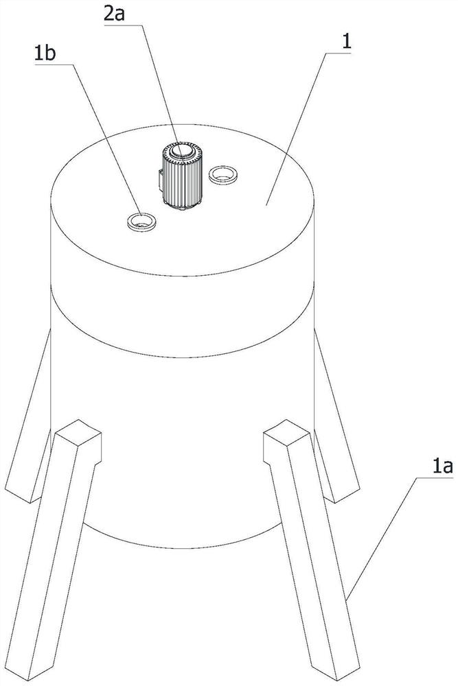
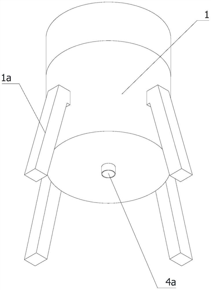
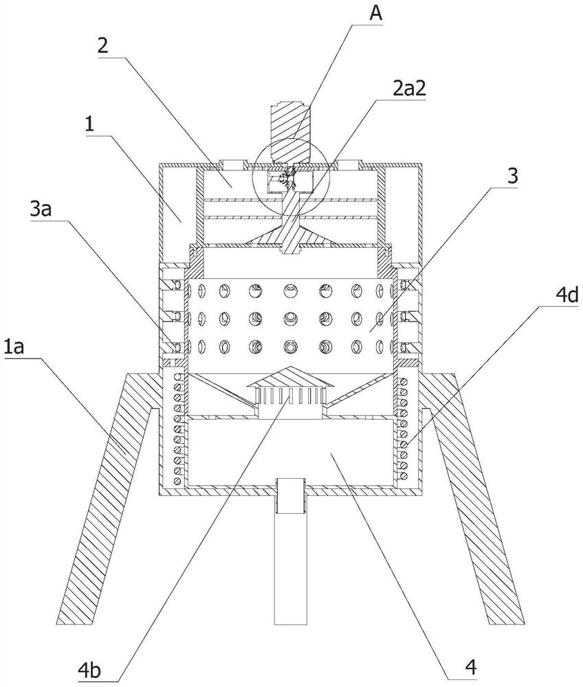
[0041] Such as Figure 1-13 Shown:

[0042]A material processing equipment for power field effect tube processing, including a support 1a and a cavity 1, the support 1a is located outside the cavity 1 and connected to the ground, and the cavity 1 is provided with a stirring chamber 2, a stirring assembly 2a, The combustion chamber 3, the heating assembly 3a and the material receiving chamber 4, the top of the chamber 1 is provided with a plurality of feeding ports 1b, the stirring assembly 2a is located in the stirring chamber 2, and the stirring assembly 2a includes a driving motor 2a1, a stirring shaft 2a2 and a stirring blade 2a3, the stirring shaft 2a2 is set in the center of the stirring chamber ...


PUM


Abstract

The invention relates to the technical field of power field-effect tube processing, in particular to material processing equipment for power field-effect tube processing, which comprises a support and a cavity, a stirring cavity, a stirring assembly, a combustion cavity, a heating assembly and a material bearing cavity are arranged in the cavity, and a plurality of feed ports are formed in the top of the cavity. The stirring assembly comprises a driving motor, a stirring shaft and stirring blades, a second filter screen is arranged between the material bearing cavity and the combustion cavity, a discharging opening is formed in the bottom of the material bearing cavity, the silicon dioxide raw material and the carbon raw material can be better mixed together through the arrangement of the stirring assembly, and the combustion efficiency is improved; meanwhile, the combustion area is increased by crushing the silicon dioxide raw material and the carbon raw material, the combustion efficiency is further improved, the energy consumption is reduced, the production efficiency of the crude silicon is improved, the purity of the crude silicon can be improved by arranging a second filter screen, and impurities in chemical reaction are reduced.

Description

technical field [0001] The invention relates to the technical field of processing power field effect tubes, in particular to a material processing device for processing power field effect tubes. Background technique [0002] Power MOS field effect transistor, that is, MOSFET, its original meaning is: MOS (MetalOxideSemiconductor Metal Oxide Semiconductor), FET (FieldEffectTransistor Field Effect Transistor), that is, the gate of the metal layer (M) is separated by the oxide layer (O). Effect to control the semiconductor (S) field effect transistor, the power field effect transistor needs to use silicon as a raw material in the process of processing, and silicon needs to be purified by processing equipment many times before it can be used, and silicon is refined when it is refined It is necessary to burn carbon and silicon dioxide to produce crude silicon through sufficient reaction. However, in the prior art, due to insufficient combustion, more energy consumption will be re...

Claims


Application Information

Patent Timeline
IPC IPC(8): B01J6/00B01F33/83C01B33/025
CPCC01B33/025B01J6/00
Inventor 焦庆
Owner 先之科半导体科技(东莞)有限公司
Why Eureka
Try Eureka