Layout and wiring method, device and equipment and readable storage medium

A technology of layout, wiring and solutions, applied in the computer field, can solve problems such as short circuit, delay, module winding congestion, increased chip power consumption, etc., and achieve the effect of solving winding congestion, reducing short circuit, and ensuring availability.

Pending Publication Date: 2022-03-08
山东云海国创云计算装备产业创新中心有限公司
View PDF0 Cites 0 Cited by
  • Summary
  • Abstract
  • Description
  • Claims
  • Application Information

AI Technical Summary

Problems solved by technology

[0002] At present, the wiring method of functional modules with complex data interaction logic usually has the following problems: the internal winding congestion of the module is serious, problems such as short circuit and time delay are prone to occur, and line resources are tight
Therefore, it is easy to cause functional errors, resulting in increased power consumption of the chip
If EDA tools are used to solve the winding problem, a certain chip area will be sacrificed

Method used


Image

  • Layout and wiring method, device and equipment and readable storage medium
  • Layout and wiring method, device and equipment and readable storage medium
  • Layout and wiring method, device and equipment and readable storage medium

Examples


Embodiment Construction

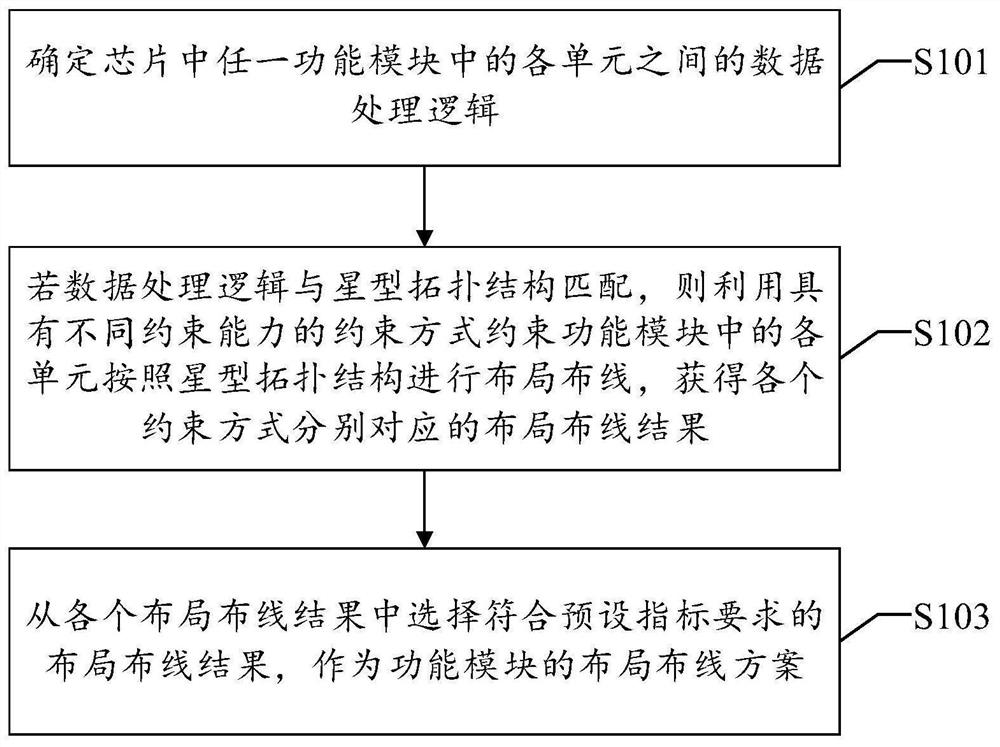
[0039] The following will clearly and completely describe the technical solutions in the embodiments of the application with reference to the drawings in the embodiments of the application. Apparently, the described embodiments are only some of the embodiments of the application, not all of them. Based on the embodiments in this application, all other embodiments obtained by persons of ordinary skill in the art without making creative efforts belong to the scope of protection of this application.

[0040] In order to introduce the present application more clearly, the technical background of the present application is introduced as follows.

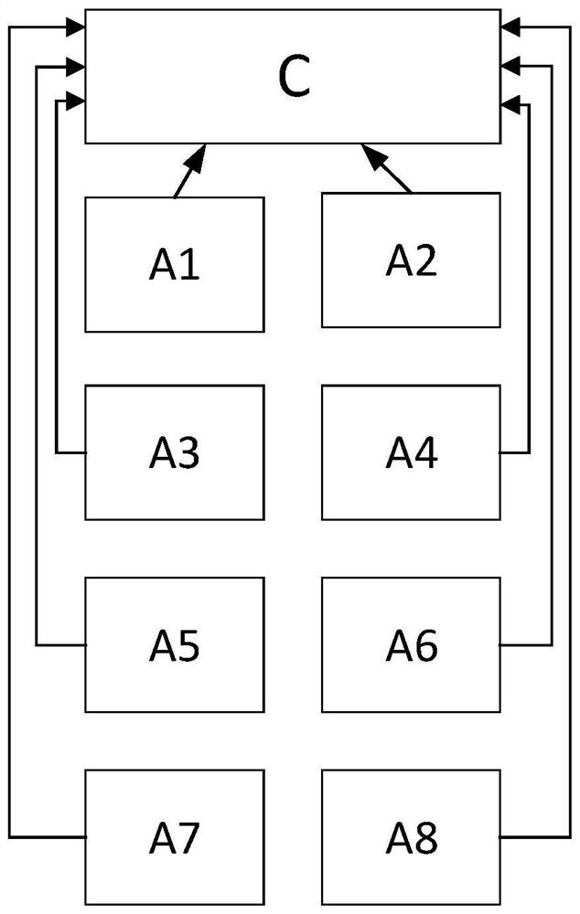
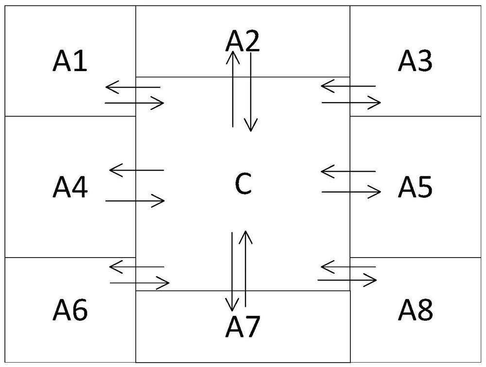
[0041] This application is optimized for chip design layout. The physical implementation of the chip design is often referred to simply as Place-and-Route (P&R). After layout and routing, continue to perform steps such as timing convergence, power consumption analysis, and manufacturability analysis on the chip, and finally convert the i...


PUM


Abstract

The invention discloses a layout and wiring method and device, equipment and a readable storage medium. According to the method and the device, for the functional module of which the data processing logic is matched with the star topology structure, the constraint modes with different constraint capabilities can be utilized to constrain each sub-module in the functional module to perform layout and wiring according to the star topology structure, so that each layout and wiring result is obtained; then, the layout wiring result meeting the preset index requirement is selected from all the layout wiring results to serve as the layout wiring scheme of the function module, layout wiring in the module can be simplified, the probability of occurrence of problems such as winding congestion, short circuit, time delay and function errors is reduced, line resources, chip power consumption and chip area are saved, and the production efficiency is improved. And a layout and wiring scheme meeting the preset index requirement can be selected, so that the performance, manufacturability and time sequence convergence effect of the chip can be improved. Correspondingly, the invention also provides a layout and wiring device, equipment and a readable storage medium, which also have the above technical effects.

Description

technical field [0001] The present application relates to the field of computer technology, in particular to a layout and wiring method, device, equipment and readable storage medium. Background technique [0002] At present, the wiring method of functional modules with complex data interaction logic usually has the following problems: the internal winding congestion of the module is serious, problems such as short circuits and time delays are prone to occur, and line resources are tight. Therefore, it is easy to cause functional errors, resulting in increased power consumption of the chip. If EDA tools are used to solve the winding problem, a certain chip area will be sacrificed. [0003] Therefore, how to simplify the layout and wiring of functional modules with complex data interaction logic is a problem to be solved by those skilled in the art. Contents of the invention [0004] In view of this, the object of the present application is to provide a layout and wiring ...

Claims


Application Information

Patent Timeline
IPC IPC(8): G06F30/392G06F30/394
CPCG06F30/392G06F30/394
Inventor 侯鹅邱进超王怡心
Owner 山东云海国创云计算装备产业创新中心有限公司
Why Eureka
Try Eureka