
Inverted Mini LED chip and manufacturing method thereof

A manufacturing method and chip technology, applied in semiconductor devices, electrical components, circuits, etc., can solve problems such as affecting product quality, short-circuiting miniLED chips, and increasing production costs, and achieve the effect of improving packaging yield and avoiding short-circuits.

Pending Publication Date: 2022-02-25
JUCAN PHOTOELECTRIC TECH (SUQIAN) CO LTD
View PDF3 Cites 0 Cited by
  • Summary
  • Abstract
  • Description
  • Claims
  • Application Information

AI Technical Summary

Problems solved by technology

However, there are still some problems in the existing technology. Due to the fluidity of the solder paste itself, the flowing solder paste contacts the pad electrodes of other chips, resulting in the phenomenon of tin connection, which further leads to a short circuit of the mini LED chip and seriously affects the product. quality, increased production costs

Method used


Image

  • Inverted Mini LED chip and manufacturing method thereof
  • Inverted Mini LED chip and manufacturing method thereof
  • Inverted Mini LED chip and manufacturing method thereof

Examples


Embodiment Construction

[0034] In order to enable those skilled in the art to better understand the technical solutions in the present application, the technical solutions in the embodiments of the present application will be clearly and completely described below in conjunction with the drawings in the embodiments of the present application. Obviously, the described The embodiments are only some of the embodiments of the present application, but not all of them. Based on the embodiments in this application, all other embodiments obtained by persons of ordinary skill in the art without creative efforts shall fall within the scope of protection of this application.

[0035] For the convenience of description, terms representing relative positions in space are used herein for description, such as "upper", "lower", "rear", "front", etc., which are used to describe the relative position of one unit or feature shown in the drawings relative to another. A unit or feature relationship. Spatially relative t...


PUM

PropertyMeasurementUnit
thicknessaaaaaaaaaa
thicknessaaaaaaaaaa
thicknessaaaaaaaaaa

Abstract

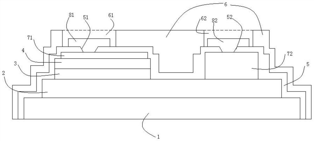
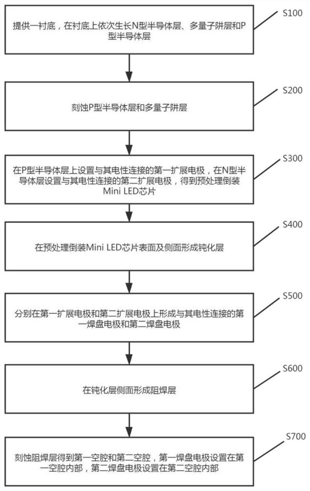
The invention provides an inverted Mini LED chip and a manufacturing method thereof. The inverted Mini LED chip comprises a substrate, an N-type semiconductor layer, a multi-quantum well layer, a P-type semiconductor layer, a passivation layer and a solder mask layer, the N-type semiconductor layer is arranged on the substrate, the multi-quantum well layer is arranged on the N-type semiconductor layer, the P-type semiconductor layer is arranged on the multi-quantum layer, the P-type semiconductor layer is provided with a first extension electrode, a second extension electrode is arranged on the N-type semiconductor layer, a first bonding pad electrode and a second bonding pad electrode are arranged on the passivation layer, the first bonding pad electrode and the second bonding pad electrode are electrically connected to the first extension electrode and the second extension electrode through through holes in the passivation layer respectively, and a solder mask layer is further arranged on the passivation layer. According to the invention, the bonding pad of the inverted mini LED chip is enclosed through the solder mask layer, solder paste is prevented from flowing, the phenomenon of tin connection is avoided, short circuit of the chip is avoided, and the packaging yield is improved.

Description

technical field [0001] The present application relates to the technical field of semiconductor light emitting devices, in particular to a flip-chip Mini LED chip and a manufacturing method thereof. Background technique [0002] Light Emitting Diode (LED), as a new type of energy-saving lighting source, has many advantages such as high energy efficiency, small size, light weight, fast response and long life, making it widely used in many fields. Among them, flip-chip LED chips are widely used because of their good heat dissipation and high reliability. The Mini LED chip has attracted more and more attention from the market due to its huge advantages in high-definition display and curved screen. [0003] The existing mini LED chip needs to be brushed with solder paste before packaging. However, there are still some problems in the existing technology. Due to the fluidity of the solder paste itself, the flowing solder paste contacts the pad electrodes of other chips, resultin...

Claims


Application Information

Patent Timeline
Patent Type & Authority Applications(China)
IPC IPC(8): H01L33/06H01L33/10H01L33/38H01L33/44H01L33/00
CPCH01L33/06H01L33/10H01L33/38H01L33/44H01L33/005
Inventor 王洪峰黄文光王世国林潇雄张振
Owner JUCAN PHOTOELECTRIC TECH (SUQIAN) CO LTD
Learn More