Medium-adjustable wave-absorbing metamaterial based on microfluidic technology and performance regulation and control device thereof
A microfluidic technology and control device technology, which is applied in laboratory containers, laboratory utensils, chemical instruments and methods, etc., can solve the problem of unpublished absorbing metamaterials and performance control devices, and it is difficult to achieve accurate absorbing performance. , real-time regulation, inability to regulate the absorbing properties of metamaterials, etc., to achieve the effect of strong designability, reducing the overall thickness, and efficient absorbing properties
- Summary
- Abstract
- Description
- Claims
- Application Information
AI Technical Summary
Problems solved by technology
Method used
Image
Examples
Embodiment 1
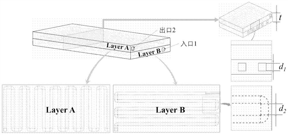
[0079] In this example, the thickness t of the printed sample is 2.4 mm, the cross-sectional shape of the microchannel is square, and d 1 is 0.6mm, and the distance between adjacent microchannels is d 2 It is 1.0mm, and the microfluidic chip is fabricated by photocuring 3D printing technology.
[0080] In this embodiment, three different solutions are selected: Pedotpss intrinsically conductive polymer solution, pure water and ethanol. The microwave absorption performance of the sample was tested by the waveguide method, and the microwave absorption rate (Absorption) test results of the intrinsically conductive polymer solution (Pedotpss), pure water (Water), and ethanol (Ethanol) in the X-band with different mass ratios were obtained. Including: Pedotpss:Water(P:W)=1:0, 1:1, 1:3; Ethanol:Water(E:W)=1:4, 1:10, and pure water W and unfilled liquid medium samples microwave absorptivity.
[0081] like Figure 4 shown, Figure 4 It is the microwave absorptivity test results o...
Embodiment 2
[0084] In this example, the thickness t of the printed sample is 2.4 mm; the cross-sectional shape of the microchannel is square, and d 1 is 0.6mm, and the distance between adjacent microchannels is d 2 0.3mm, 0.5mm, 0.75mm, 1.0mm, 1.5mm, and 1.75mm, respectively. The microfluidic chip is prepared by photocuring 3D printing technology. Pure water was injected into all samples in this example as a microwave loss medium. The wave-absorbing properties of the samples were tested by the waveguide method, and the experimental results are shown in the attached Figure 5 shown, Figure 5 is the distance d between adjacent microfluidic channels according to embodiments of the present disclosure 2 The microwave absorptivity test results in the X-band of samples of 0.3mm, 0.5mm, 0.75mm, 1.0mm, 1.5mm, and 1.75mm, respectively. The results show that by adjusting the distance between adjacent microchannels, the microwave absorption peak of the microfluidic chip can be moved in the enti...
PUM
| Property | Measurement | Unit |
|---|---|---|
| thickness | aaaaa | aaaaa |
Abstract
Description
Claims
Application Information
 - Generate Ideas
- Intellectual Property
- Life Sciences
- Materials
- Tech Scout
- Unparalleled Data Quality
- Higher Quality Content
- 60% Fewer Hallucinations
Browse by: Latest US Patents, China's latest patents, Technical Efficacy Thesaurus, Application Domain, Technology Topic, Popular Technical Reports.
© 2025 PatSnap. All rights reserved.Legal|Privacy policy|Modern Slavery Act Transparency Statement|Sitemap|About US| Contact US: help@patsnap.com


