Chip detection equipment for chip processing and production

A chip detection and chip technology, which is applied in the field of chip detection equipment for chip processing and production, can solve problems such as affecting detection accuracy, and achieve the effect of solving easy displacement, easy positioning, and not easy to offset.

Pending Publication Date: 2022-01-28
KINGDOM AUTO CONTROL TECH LTD CHANGSHA
View PDF0 Cites 0 Cited by
  • Summary
  • Abstract
  • Description
  • Claims
  • Application Information

AI Technical Summary

Problems solved by technology

[0004] The embodiment of the present application provides a chip detection device for chip processing and production, which solves the problem of manual detection of chips in the prior art, which affects the detection accuracy, and realizes the effect of automatic detection of chips and improvement of detection accuracy.

Method used


Image

  • Chip detection equipment for chip processing and production
  • Chip detection equipment for chip processing and production
  • Chip detection equipment for chip processing and production

Examples


Embodiment Construction

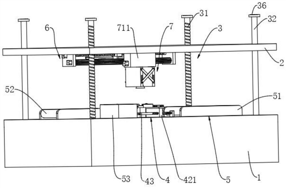
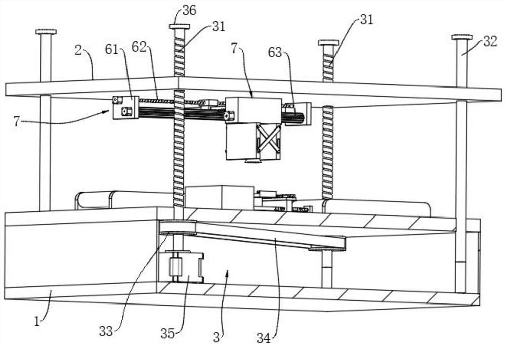
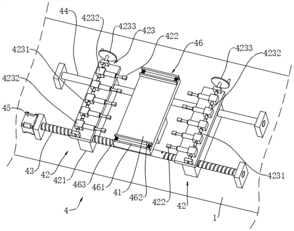
[0027] The embodiment of the present application provides a chip detection device for chip processing and production, drives the clamping device 7 to move to the position of the chip through the moving device 6, and uses the clamping device 7 to clamp the chip to the detection device 4 to detect the chip For qualified chips, the chips are placed on the transfer device 5 through the clamping device 7 for transmission, and for unqualified chips, the chips are placed in the recycling box 53 through the clamping device 7 for recycling, which solves the problem of manual detection in the prior art. The chip, which affects the detection accuracy, has realized the effect of automatically detecting the chip and improving the detection accuracy.

[0028] In order to better understand the above-mentioned technical solution, the above-mentioned technical solution will be described in detail below in conjunction with the accompanying drawings and specific implementation methods.

[0029] ...


PUM


Abstract

The invention relates to the technical field of chip production, and discloses chip detection equipment for chip processing and production, the chip detection equipment comprises a base and a top plate arranged above the base, and the base and the top plate are connected through a lifting device; a detection device and transmission devices are arranged on the base; the transmission devices are located on the two sides of the detection device. a clamping device and a moving device for driving the clamping device to move are arranged on the top plate; and the clamping device comprises a clamping mechanism connected with the moving device and an adsorption mechanism arranged on the clamping mechanism. The chip detection equipment has the effect of improving the detection accuracy.

Description

technical field [0001] The invention relates to the technical field of chip production, in particular to a chip detection device for chip processing and production. Background technique [0002] A chip generally refers to the carrier of an integrated circuit, and is also the result of the design, manufacture, packaging, and testing of an integrated circuit. It is usually an independent whole that can be used immediately. An electronic chip is a miniature electronic device or component. It uses a certain process to interconnect the transistors, resistors, capacitors, inductors and other components and wiring required in a circuit, and makes them on a small or several small semiconductor chips or chips. Dielectric substrate, and then packaged in a package, to become a microstructure with the required circuit functions; all the components have been integrated in the structure, making electronic components towards miniaturization, low power consumption, intelligence and high rel...

Claims


Application Information

Patent Timeline
IPC IPC(8): H01L21/68H01L21/683H01L21/687H01L21/66
CPCH01L21/6838H01L21/68721H01L21/68764H01L21/68H01L21/68742H01L22/10
Inventor 龙天瑞华传健陈奇志
Owner KINGDOM AUTO CONTROL TECH LTD CHANGSHA
Why Eureka
Try Eureka