FPGA life test method
A life test and multiplier technology, applied in the field of FPGA life test, can solve the problems of initial fatal failure and early life failure
- Summary
- Abstract
- Description
- Claims
- Application Information
AI Technical Summary
Problems solved by technology
Method used
Image
Examples
Embodiment 1
[0022] A kind of FPGA life test method of the present embodiment, carries out following steps:
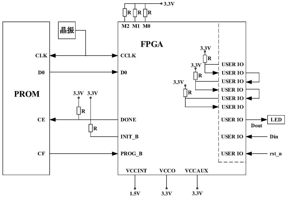
[0023] 1) Set various configurations of the life test circuit;
[0024] These include the selection of life test circuit configuration mode, the processing method of programmable logic resources, the processing method of embedded multiplier, the processing method of block memory, and the processing method of user IO;
[0025] 2) Set the external excitation conditions required for the test;
[0026] Including, life test voltage, input terminal requirements, output terminal requirements, input signal requirements, amplitude, resistance R, input excitation signal, logic output signal;
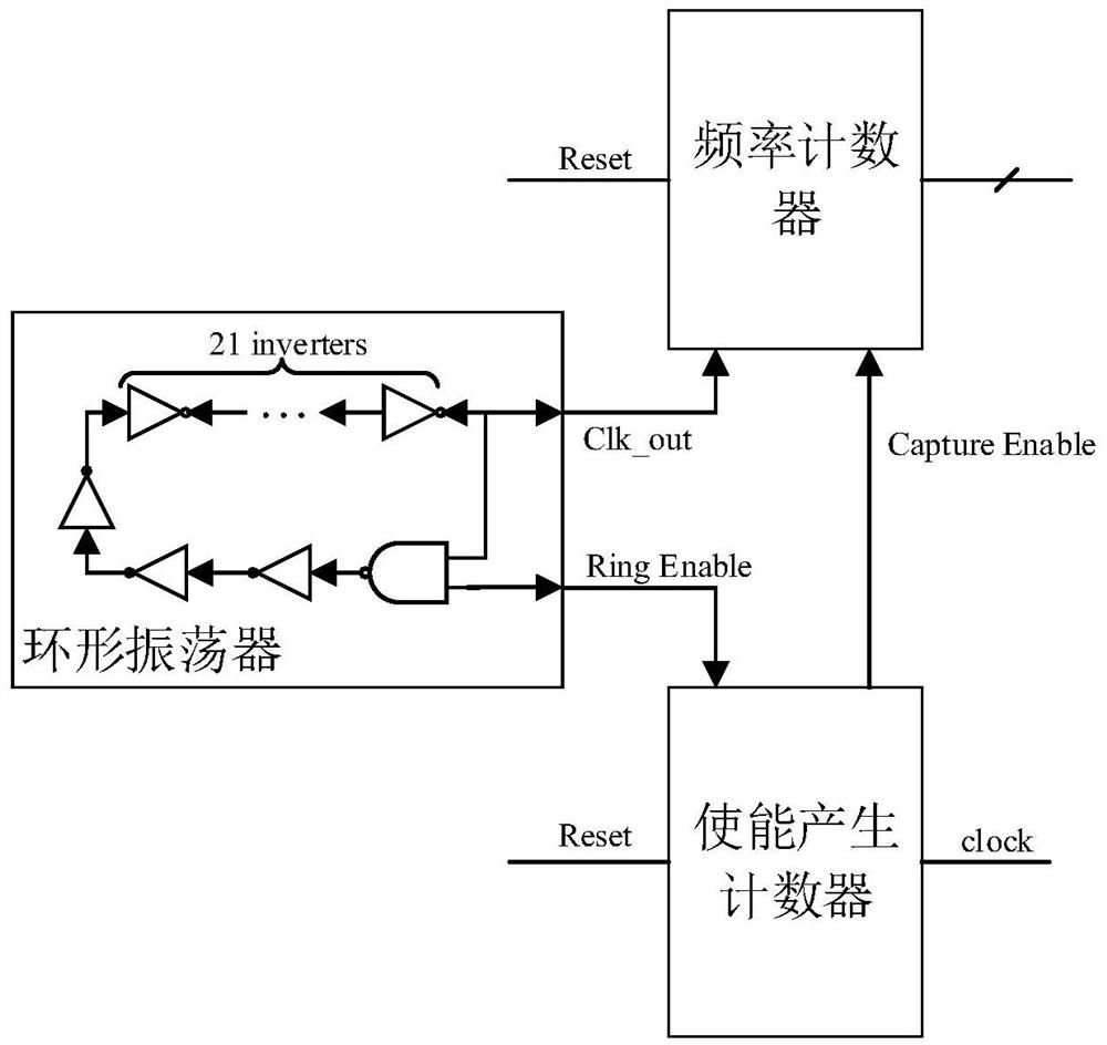
[0027] 3) Use the interpolation ring oscillator circuit to measure the junction temperature of the device to realize feedback modification and iterative optimization of the input clock operating frequency, and monitor the status of the device during the life test through the LED status indicator conne...
PUM
 Abstract
Description
Claims
Application Information
 - R&D
- Intellectual Property
- Life Sciences
- Materials
- Tech Scout
- Unparalleled Data Quality
- Higher Quality Content
- 60% Fewer Hallucinations
Browse by: Latest US Patents, China's latest patents, Technical Efficacy Thesaurus, Application Domain, Technology Topic, Popular Technical Reports.
© 2025 PatSnap. All rights reserved.Legal|Privacy policy|Modern Slavery Act Transparency Statement|Sitemap|About US| Contact US: help@patsnap.com


