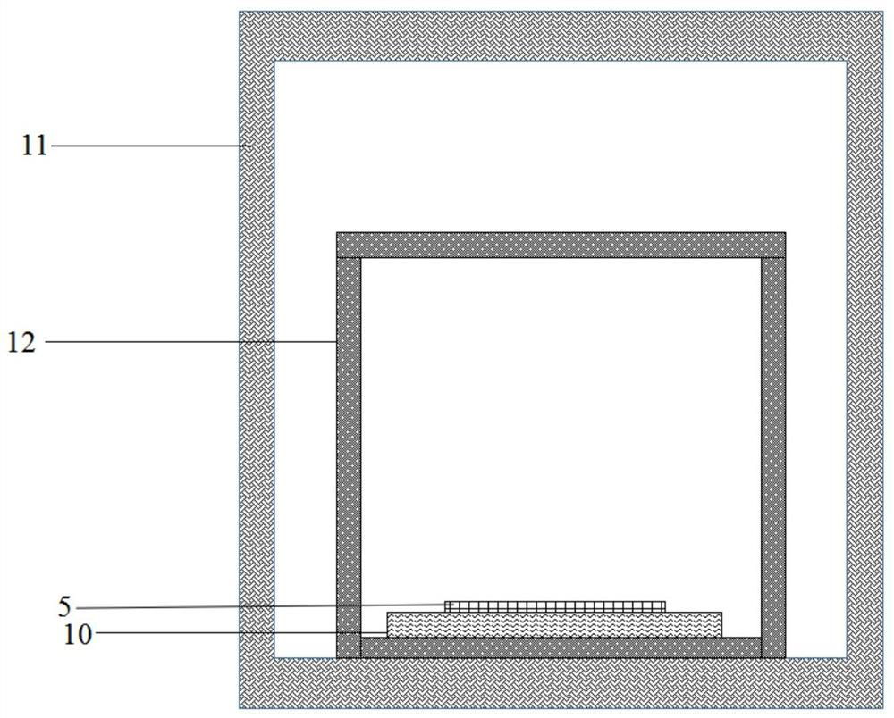
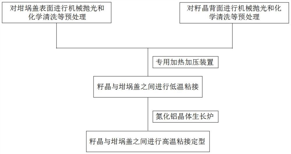
Seed crystal high-temperature bonding equipment for aluminum nitride crystal growth and method thereof
A technology of crystal growth and bonding method, which is applied in the directions of crystal growth, single crystal growth, single crystal growth, etc. It can solve the problems of loss of seed crystal surface, small radial and axial temperature gradient, and crystal quality deterioration, etc., to achieve Increase usable area, achieve low cost, avoid degraded effect
- Summary
- Abstract
- Description
- Claims
- Application Information
AI Technical Summary
Problems solved by technology
Method used
Image
Examples
Embodiment 1
[0042] Embodiment 1: bonding silicon carbide seed crystals in an induction heating furnace.
[0043] Concrete preparation process is as follows:
[0044] (1) Select a suitable size tantalum carbide crucible cover and silicon carbide seed crystal, and perform pretreatments such as mechanical polishing and chemical cleaning on the crucible cover. The surface roughness Ra value is required to be 1.5 μm, and the flatness tolerance level is 3. At the same time, pretreatments such as chemical polishing and chemical cleaning are carried out on the back of the seed crystal, and the RMS value of the atomic microscope surface roughness is required to be 9nm.
[0045] (2) Place the seed crystal on the crucible cover, put the crucible cover down on the sample stage of the special heating and pressurizing device, place a sapphire wafer with an unpolished surface on the front of the seed crystal, and operate the pressure transmission device to lower slowly Press on the sapphire wafer, star...
Embodiment 2
[0048] Embodiment 2: bonding aluminum nitride seed crystals in an induction heating furnace.
[0049] Concrete preparation process is as follows:
[0050] (1) Select a suitable size tantalum carbide crucible cover and silicon carbide seed crystal, and perform pretreatments such as mechanical polishing and chemical cleaning on the crucible cover. The surface roughness Ra value is required to be 1.3 μm, and the flatness tolerance level is 3. At the same time, pretreatments such as chemical polishing and chemical cleaning are carried out on the back of the seed crystal, and the RMS value of the atomic microscope surface roughness is required to be 7nm.
[0051] (2) Place the seed crystal on the crucible cover, place the crucible cover on the sample stage of the special heating and pressurizing device, place a boron nitride wafer with an unpolished surface on the front of the seed crystal, and operate the pressure transmission device slowly Drop the pressure on the boron nitride ...
Embodiment 3
[0054] Embodiment 3: bonding aluminum nitride seed crystals in a resistance heating furnace.
[0055] Concrete preparation process is as follows:
[0056] (1) Select a suitable size tantalum carbide crucible cover and silicon carbide seed crystal, and perform pretreatments such as mechanical polishing and chemical cleaning on the crucible cover. The surface roughness Ra value is required to be 1.2 μm, and the flatness tolerance level is 3. At the same time, pretreatments such as chemical polishing and chemical cleaning are carried out on the back of the seed crystal, and the RMS value of the atomic microscope surface roughness is required to be 5nm.
[0057] (2) Place the seed crystal on the crucible cover, put the crucible cover down on the sample stage of the special heating and pressurizing device, place a sapphire wafer with an unpolished surface on the front of the seed crystal, and operate the pressure transmission device to lower slowly Press on the sapphire wafer, sta...
PUM
| Property | Measurement | Unit |
|---|---|---|
| surface roughness | aaaaa | aaaaa |
| surface roughness | aaaaa | aaaaa |
| surface roughness | aaaaa | aaaaa |
Abstract
Description
Claims
Application Information
 - Generate Ideas
- Intellectual Property
- Life Sciences
- Materials
- Tech Scout
- Unparalleled Data Quality
- Higher Quality Content
- 60% Fewer Hallucinations
Browse by: Latest US Patents, China's latest patents, Technical Efficacy Thesaurus, Application Domain, Technology Topic, Popular Technical Reports.
© 2025 PatSnap. All rights reserved.Legal|Privacy policy|Modern Slavery Act Transparency Statement|Sitemap|About US| Contact US: help@patsnap.com


