Eureka AIR delivers breakthrough ideas for toughest innovation challenges, trusted by R&D personnel around the world.

Lithium niobate film electro-optical modulator and preparation method thereof

An electro-optic modulator, lithium niobate technology, applied in the field of optical communication, can solve the problems of high cost, large electrode spacing, and affecting the performance of the modulator, and achieve the effect of increasing the overlapping area, reducing the process cost, and increasing the effective refractive index

Pending Publication Date: 2022-01-07
NANJING NANZHI INST OF ADVANCED OPTOELECTRONIC INTEGRATION NANJING
View PDF0 Cites 0 Cited by
  • Summary
  • Abstract
  • Description
  • Claims
  • Application Information

AI Technical Summary

Problems solved by technology

[0006] In order to solve the problems existing in the background technology, the present invention proposes a lithium niobate thin film electro-optic modulator with a special structure and its preparation method, which effectively solves the high cost and high cost caused by the large lithium niobate thin film etching area. The contradiction between the electrode spacing is too large and the performance of the modulator is affected

Method used


Image

  • Lithium niobate film electro-optical modulator and preparation method thereof
  • Lithium niobate film electro-optical modulator and preparation method thereof
  • Lithium niobate film electro-optical modulator and preparation method thereof

Examples


Embodiment 1

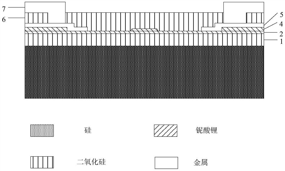
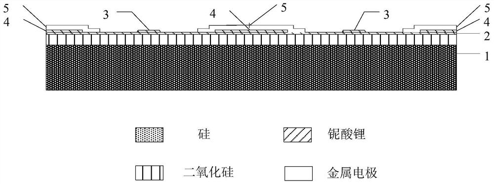
[0039] Such as figure 1 As shown, this embodiment includes a substrate wafer 1, a lithium niobate thin film substrate 2, a lithium niobate optical waveguide 3, a lithium niobate thin film lining 4, a traveling wave electrode 5, a protective layer 6 and an extraction electrode 7. The extraction electrode 7 is connected to the traveling wave electrode 4 . Among them, the traveling wave electrode structure in the lithium niobate thin film electro-optic modulator is as follows figure 2 There are three traveling-wave electrodes 5 as shown, which are respectively located on both sides and the center above the lithium niobate film substrate 2, and the lithium niobate film lining 4 is located between the lithium niobate film substrate 2 and the traveling-wave electrode. 5, the area of ​​the traveling wave electrode 5 is larger than the area of ​​the lithium niobate thin film lining 4 so as to completely cover the lithium niobate thin film lining 4.

[0040] The specific implementat...


PUM

PropertyMeasurementUnit
Widthaaaaaaaaaa
Lengthaaaaaaaaaa
Thicknessaaaaaaaaaa

Abstract

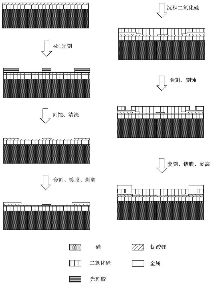
The invention discloses a lithium niobate film electro-optical modulator which comprises a substrate wafer (1), a lithium niobate film substrate (2), a lithium niobate optical waveguide (3), a lithium niobate film lining (4), a traveling wave electrode (5), a protective layer (6) and an extraction electrode (7). By improving the structure of a traveling wave electrode in electro-optic modulator in general design, a part of the metal electrode (5) covers an etching area, and a part of the metal electrode (5) covers the lithium niobate film lining (4), so that the effective refractive index of microwaves is increased under the condition that the distance between the electrodes is the same, the wave velocity matching is realized, and the bandwidth of the electro-optical modulator is improved. The invention further provides a preparation method of the lithium niobate film electro-optical modulator; the lithium niobate film is directly etched to obtain the required waveguide structure based on the traveling wave electrode structure in the lithium niobate film electro-optical modulator, the etching area is reduced, and the process difficulty and cost are reduced.

Description

technical field [0001] The present application relates to the technical field of optical communication, in particular to a lithium niobate thin film electro-optical modulator and a preparation method thereof. Background technique [0002] Electro-optic modulators are widely used in optical fiber communication, optical fiber sensing, microwave photonics, quantum communication and other technical fields. A key function of optical fiber for low-loss transmission. The external modulator using the principle of linear electro-optic effect of lithium niobate crystal has an important application in optical fiber signal transmission system due to its outstanding advantages such as low chirp coefficient, high modulation bandwidth, and high on-off extinction ratio. [0003] In recent years, with the maturity of large-size and high-quality lithium niobate thin film materials, lithium niobate thin film electro-optic modulator chips fabricated on lithium niobate thin film wafers using CM...

Claims


Application Information

Patent Timeline
IPC IPC(8): G02F1/035G02F1/03G02F1/21G02F1/225G02B6/136G03F7/00
CPCG02F1/035G02F1/0316G02F1/212G02F1/225G02B6/136G03F7/00
Inventor 尹志军叶志霖崔国新许志城
Owner NANJING NANZHI INST OF ADVANCED OPTOELECTRONIC INTEGRATION NANJING
Why Eureka
Eureka Blog
Learn More