Shell assembly of high-speed optical signal transmitting device and high-speed optical signal transmitting device

A technology for transmitting devices and housing components, which is applied in the field of housing components and high-speed optical signal transmitting devices, which can solve the problems of long wiring, affecting the performance of optical transmitting devices, reducing the operating bandwidth of driving chips and semiconductor lasers, and reducing the overall Low cost, reduced thermal interference, and simple structure

Inactive Publication Date: 2021-12-24
成都英思嘉半导体技术有限公司
View PDF10 Cites 2 Cited by
  • Summary
  • Abstract
  • Description
  • Claims
  • Application Information

AI Technical Summary

Problems solved by technology

[0004] The purpose of the present invention is: for the semiconductor laser (LD) and the driver chip (Driver) that exist in the prior art, the wiring is very long, and the long high-frequency signal wiring is easy to generate parasitic inductance, and the impact of parasitic capacitance and impedance mismatch is high. In order to solve the problem of high-frequency signal quality, reduce the operating bandwidth of the driver chip and semiconductor laser, and affect the performance of the optical emitting device, a housing assembly and a high-speed optical signal emitting device for the high-speed optical signal emitting device are provided, which will drive the chip (Driver) It is placed adjacent to the semiconductor laser (LD) and packaged together in the housing of the light-emitting device, so as to shorten the lead length between the driver chip and the semiconductor laser as much as possible, and improve the quality of high-frequency signals

Method used


Image

  • Shell assembly of high-speed optical signal transmitting device and high-speed optical signal transmitting device
  • Shell assembly of high-speed optical signal transmitting device and high-speed optical signal transmitting device
  • Shell assembly of high-speed optical signal transmitting device and high-speed optical signal transmitting device

Examples


Embodiment 1

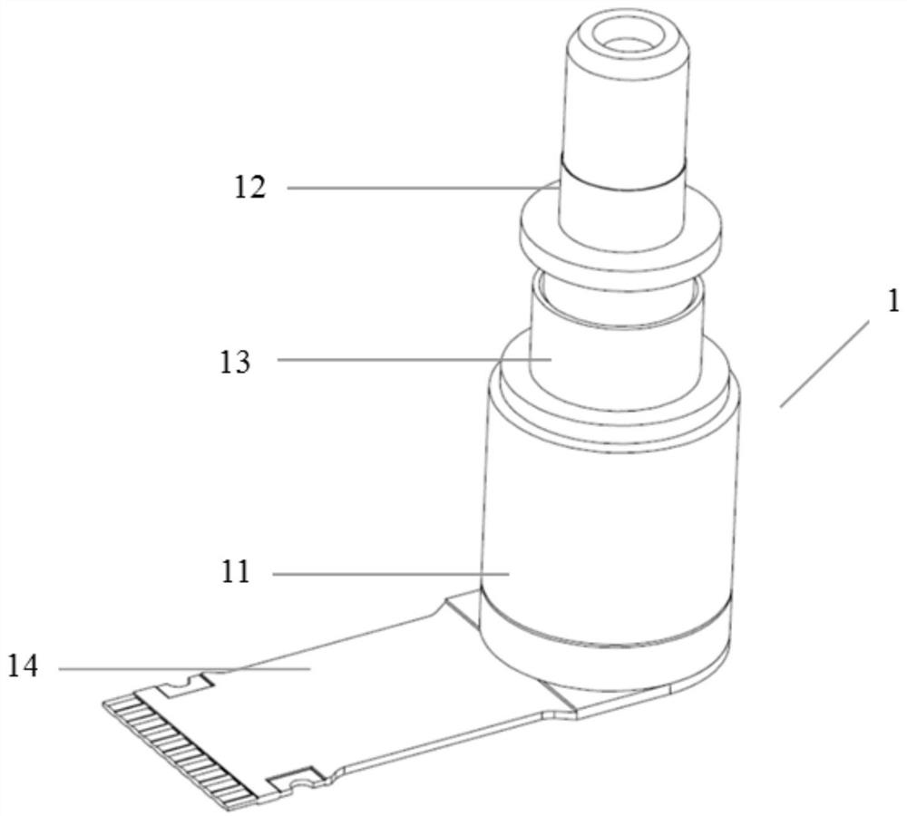
[0043] The light-emitting device 1 provided by the present invention operates at a rate of 25Gb / s and above, and mainly includes 4 components, a housing TO-CAN 11, a connector Receptacle 12, a mounting ring Z-ring 13 and a flexible circuit board FPC 14, a The appearance of the light-emitting device is as figure 1 shown. The housing TO-CAN 11 is used to package electronic components and optical devices; the connector Receptacle 12 is used to connect with the external optical fiber connector 2; the installation ring Z-ring 13 is used for the connection between the connector Receptacle 12 and the housing TO-CAN 11 Coupling welding; the flexible circuit board FPC 14 is used to connect the main board 31 of the optical transceiver module 3 .

[0044] The use mode of the light emitting device 1 is placed in the optical transceiver module 3 for the emission of optical signals, and the use mode of the light emitting device is as follows: figure 2 shown. One end of the connector Rec...

Embodiment 2

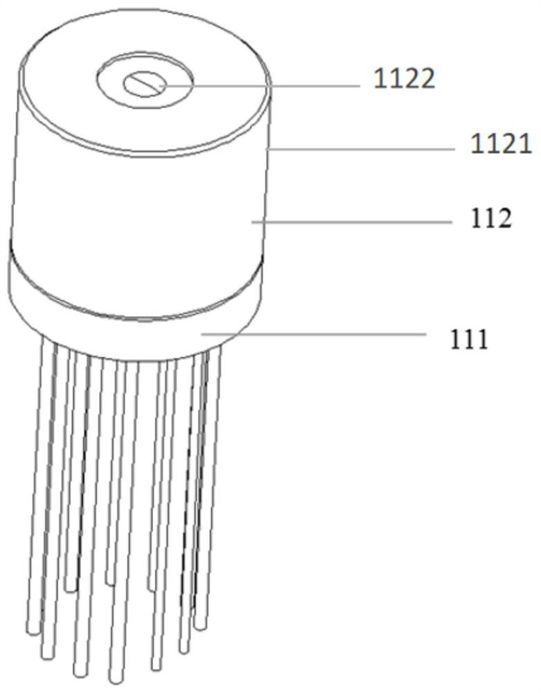
[0053] The TO-Header 111 and the TO-Cap 112 of the housing TO-CAN of the light-emitting device 1 embodiment 2 provided by the present invention are the same as those in Example 1, as image 3 , Figure 4 , Figure 5 shown. The schematic diagram of the components inside the shell TO-CAN is as follows: Figure 11 shown. A heat sink substrate 1131 is placed on the TO-Header 111 . The laser 1132 and the driving chip 1133 are placed adjacent to each other and installed on the heat sink substrate 1131 . A heating resistor 1134 is also placed on the heat sink substrate 1131 .

[0054] The heat sink substrate 1131 is pasted on the header TO-Header 111 by glue, the semiconductor laser LD 1132 is welded or glued on the conductive pattern 11311 on the surface of the heat sink substrate 1131 by gold-tin soldering, and the driver chip 1133 is also pasted on the conductive pattern 1131 by conductive glue. heat sink on the substrate 1131 . A photodetector 1142 is mounted on the side f...


PUM


Abstract

The invention relates to a shell assembly of a high-speed optical signal transmitting device and the high-speed optical signal transmitting device. The shell assembly comprises a shell, a heat sink substrate, a laser and a driving chip, the heat sink substrate, the laser and the driving chip are packaged in the shell, and the laser and the driving chip are adjacently placed on the heat sink substrate according to the axis direction of the shell. The driving chip and the laser are adjacently arranged on the heat sink substrate and packaged in the shell, so that a connecting line of the driving chip and the laser is as short as possible, long wiring between the driving chip and a semiconductor laser is avoided, the parasitic inductance and the parasitic capacitance caused by the long wiring are reduced, and the use bandwidth of a light emitting device is improved, so that the high-speed optical signal transmitting device can easily work at the speed of 25Gb / s and above, and is more suitable for being applied to the high-speed optical communication devices. Meanwhile, a non-turning linear light path design is adopted, a part of light turning elements and procedures are reduced, and the cost of the high-speed optical signal transmitting device is effectively reduced.

Description

technical field [0001] The invention relates to the technical field of laser diodes, in particular to a casing assembly of a high-speed optical signal transmitting device and a high-speed optical signal transmitting device. Background technique [0002] At present, the high-speed optical signal transmitting device (TOSA) and the driver chip (Driver) of the semiconductor laser (LD) commonly used in the optical transceiver module for high-speed optical fiber communication are arranged on the circuit board main board of the optical transceiver module. The driver chip (Driver) is connected to the light-emitting device (TOSA) through a flexible circuit board (FPC), and drives the semiconductor laser (LD) in the light-emitting device (TOSA). The main function of the driver chip (Driver) is to couple the DC bias current of the semiconductor laser (LD) with the high-frequency modulation current, and provide the modulated driving current for the semiconductor laser (LD). At the same...

Claims


Application Information

Patent Timeline
Patent Type & Authority Applications(China)
IPC IPC(8): H01S5/02212H01S5/023H01S5/02315H01S5/02345H01S5/024H04B10/50
CPCH01S5/02212H01S5/023H01S5/02315H01S5/02345H01S5/024H01S5/02453H01S5/02469H04B10/503
Inventor 鞠兵维卡斯·马南赖人铭
Owner 成都英思嘉半导体技术有限公司
Why Eureka
Try Eureka