Circuit board manufacturing method for processing electroplated hole and anti-corrosion pattern by laser
A circuit board method and anti-etching pattern technology, which is applied in the direction of chemical/electrolytic method to remove conductive materials, printed circuit, pattern and photolithography, etc., to achieve the effect of shortening the manufacturing process, fewer steps and high efficiency
- Summary
- Abstract
- Description
- Claims
- Application Information
AI Technical Summary
Problems solved by technology
Method used
Image
Examples
Embodiment 1
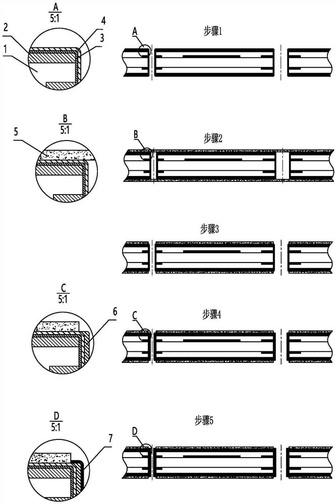
[0076] Copper-clad laminates are commonly used as the basic material to make circuit boards in the electronics industry. The copper-clad laminates include an insulating substrate 1 and a copper-clad laminate copper layer 2 .
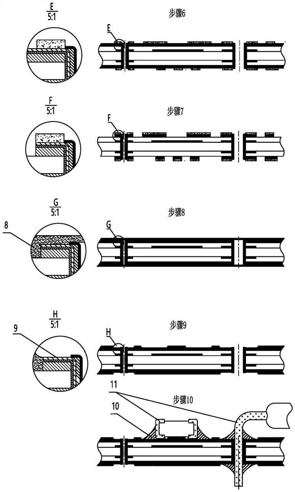
[0077] This embodiment takes a double-sided printed circuit board as an example, and the specific processing steps are as follows:
[0078] (1) The circuit board base material copper clad laminate includes an insulating substrate 1 and a copper clad laminate 2. The copper clad laminate is drilled, and the initial conductive layer 3 is deposited on the product in process of the double-sided circuit board that has been drilled, and the copper is electroplated to The thickness can withstand subsequent processes to form electroplated thin copper 4 .
[0079] The purpose of making thin copper on the initial conductive layer is to increase the reliability of the manufacturing process, and its thickness should reach the lower limit to ensure the reliability of ...
Embodiment 2
[0114] Copper-clad laminates are commonly used as the basic material to make circuit boards in the electronics industry. The copper-clad laminates include an insulating substrate 1 and a copper-clad laminate copper layer 2 .
[0115] In this embodiment, a four-layer circuit board whose inner circuit has been fabricated is taken as an example, and the specific processing steps are as follows:
[0116] (1) The circuit board base material copper-clad laminate includes an insulating substrate 1 and a copper-clad laminate copper layer 2. The drilled copper-clad laminate is completed, and the initial conductive layer 3 is deposited on the finished product of the four-layer circuit board that has been drilled, and copper is electroplated to The thickness can withstand subsequent processes to form electroplated thin copper 4 .
[0117] Electroless copper is deposited on the four-layer circuit board that has been drilled and the inner layer circuit is completed, and copper is electropl...
PUM
| Property | Measurement | Unit |
|---|---|---|
| Thickness | aaaaa | aaaaa |
| Thickness | aaaaa | aaaaa |
| Thickness | aaaaa | aaaaa |
Abstract
Description
Claims
Application Information
 - R&D
- Intellectual Property
- Life Sciences
- Materials
- Tech Scout
- Unparalleled Data Quality
- Higher Quality Content
- 60% Fewer Hallucinations
Browse by: Latest US Patents, China's latest patents, Technical Efficacy Thesaurus, Application Domain, Technology Topic, Popular Technical Reports.
© 2025 PatSnap. All rights reserved.Legal|Privacy policy|Modern Slavery Act Transparency Statement|Sitemap|About US| Contact US: help@patsnap.com


