CMOS SPAD photoelectric device with deep N well in reverse doping distribution

A technology of optoelectronic devices and reverse doping, applied in electrical components, semiconductor devices, circuits, etc., can solve problems such as being unfavorable to improve device noise performance, band-band tunneling effect, and increasing device dark current value.

Inactive Publication Date: 2021-11-16
重庆亚川电器有限公司
View PDF0 Cites 1 Cited by
  • Summary
  • Abstract
  • Description
  • Claims
  • Application Information

AI Technical Summary

Problems solved by technology

[0004] (However, the use of this technology makes the photogenerated carriers prone to band tunneling effect in the event of avalanche breakdown of the device, increasing the value of the dark current of the device, which is not conducive to improving the noise performance of the device

Method used


Image

  • CMOS SPAD photoelectric device with deep N well in reverse doping distribution
  • CMOS SPAD photoelectric device with deep N well in reverse doping distribution
  • CMOS SPAD photoelectric device with deep N well in reverse doping distribution

Examples


Embodiment Construction

[0020] The technical solutions in the embodiments of the present invention will be described in detail below with reference to the drawings in the embodiments of the present invention. The described embodiments are merely a part of the embodiments of the invention.

[0021] The technical solution to solve the above technical problem is:

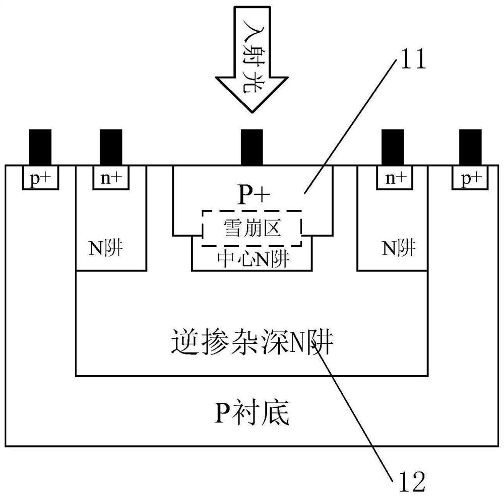
[0022] Such as figure 1 The structure diagram showing the new CMOS SPAD photoelectric device. As can be seen from the figure, the device is a planar structure composed of a P + / central N-well / inverse doped depth N well / P substrate. Where the P + / Central N well constitutes a avalanche region (corresponding to the 11 region), the optical carrier has a collision ionization in this region to increase, thereby forming a naked eye to be observed to achieve photoelectric conversion. The photon absorbing region (corresponding to the 12 region) of the counter-doped deep N well constitutes the device, and the reverse doping means that the deep N we...


PUM

PropertyMeasurementUnit
Thicknessaaaaaaaaaa

Abstract

The invention relates to a CMOS SPAD photoelectric device with a deep N well in reverse doping distribution. The CMOS SPAD photoelectric device comprises a P substrate, the deep N well, a central N well and a P + layer are arranged on the P substrate, N wells are arranged at the two sides of the deep N well, the deep N well is of a reverse doping distribution structure, namely, the concentration of the deep N well close to the surface of the device is low, and the concentration of the deep N well is higher with the longitudinal depth away from the surface of the device is increased, transverse diffusion exists between the N wells at the two sides in the deep N well and the central N well, an n-virtual protection ring is formed at the edge of the PN junction, when incident photons are emitted into the device and are mainly absorbed by the deep N well, most photons can be utilized by the P + layer / central N well junction to form photon-generated carriers, and only a small number of photons penetrate through the deep N well to form a photon-generated carrier on the P substrate. The photon detection efficiency of the device is improved mainly from two aspects of increasing the thickness of the absorption region of the device and optimizing the quantum efficiency of the device.

Description

Technical field [0001] The present invention belongs to the semiconductor photodetection and sensing field, and the structure of the APD photoelectric device, and more particularly to a design of a CMOS SPAD photoelectric device having high photon detection efficiency. Background technique [0002] Single Photo Avalanche DioDe is widely used in the field of automotive electronics, three-dimensional imaging, instrumentation, bioconics, fluorescent life imaging, etc. due to its characteristics of single photon sensitivity, and is a work in the cover. The semiconductor optoelectronic detector using a PN junction structure under the leather mode (the anti-bias voltage is greater than the breakdown voltage). When the photon is irradiated into the PN, the light carrier is accelerated to move to the avalante and produce a multiplication effect such that the single photon can trigger a large current pulse signal. With the expansion of the application, the performance requirements of SPAD...

Claims


Application Information

Patent Timeline
IPC IPC(8): H01L31/107H01L31/0352
CPCH01L31/107H01L31/035272
Inventor 张瑜殷文兵
Owner 重庆亚川电器有限公司
Why Eureka
Try Eureka