Flip LED chip and production method thereof

A LED chip and flip-chip technology, which is applied in the direction of electrical components, circuits, semiconductor devices, etc., can solve the problems of reducing product reliability, easy to fall off, and high refractive index of GaN, so as to increase contact ability, improve brightness and current resistance. Effect

Active Publication Date: 2021-11-12
XIAMEN SILAN ADVANCED COMPOUND SEMICON CO LTD
View PDF19 Cites 0 Cited by
  • Summary
  • Abstract
  • Description
  • Claims
  • Application Information

AI Technical Summary

Problems solved by technology

However, the front-mounted light-emitting diodes have the following disadvantages: first, the GaN surface emits light, the GaN refractive index is high, and the total reflection angle of the emitted light is small, resulting in a decrease in the external quantum efficiency of GaN-based light-emitting diodes; The thermal conductivity is poor, and the heat generated during the light-emitting process of the LED cannot be effectively exported, which reduces the reliability of the product
[0005] The flip-chip DBR mirror process uses ITO (Indium Tin Oxides, indium tin oxide) as the current spreading layer, the DBR mirror has high reflectivity, high brightness, and is compatible with other films Strong adhesion of layers, but uneven current spreading
Flip-chip metal mirror technology uses silver (Ag) mirror as the current spreading layer. The metal has strong current spreading ability, but its adhesion to other film layers is weak and it is easy to fall off.
For the flip-chip metal mirror process, in order to increase the adhesion, a transparent adhesive layer (that is, the middle adhesive metal layer) is usually added between the metal reflective layer and the lower film layer, but the increase of the adhesive layer greatly reduces the The reflectivity of the metal reflective layer affects the brightness of the LED

Method used


Image

  • Flip LED chip and production method thereof
  • Flip LED chip and production method thereof
  • Flip LED chip and production method thereof

Examples


Embodiment Construction

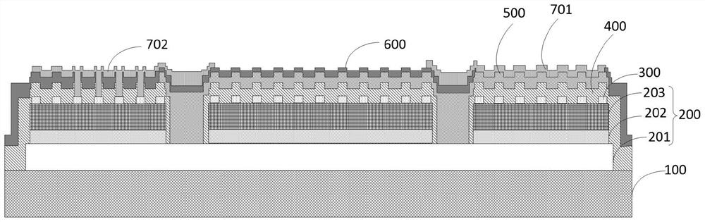
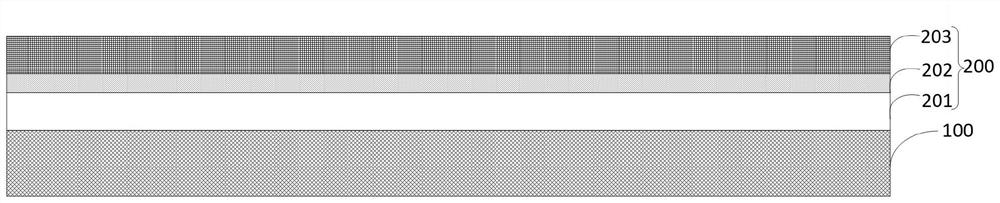
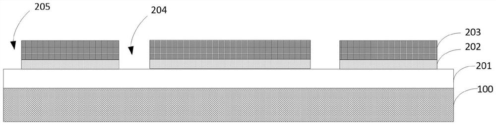
[0065] Flip-chip light-emitting diodes can be divided into two processes, namely the flip-chip DBR reflector process and the flip-chip metal reflector process. The flip-chip DBR mirror process uses ITO (Indium Tin Oxides, indium tin oxide) as the current spreading layer. The DBR mirror has high reflectivity, high brightness, and strong adhesion to other film layers, but the current spread is uneven. The flip-chip metal mirror technology uses a silver (Ag) mirror as the current spreading layer. The metal has a strong current spreading ability, but its adhesion to other film layers is weak, and it is easy to fall off. For the flip-chip metal mirror process, in order to increase the adhesion, a transparent adhesive layer is usually added between the metal reflective layer and the underlying film layer, but the increase of the adhesive layer greatly reduces the reflectivity of the metal reflective layer.

[0066] In order to make full use of the advantages of the flip-chip DBR and...


PUM

PropertyMeasurementUnit
diameteraaaaaaaaaa
thicknessaaaaaaaaaa
thicknessaaaaaaaaaa

Abstract

The invention provides a flip LED chip and a production method thereof. The flip LED chip comprises: a substrate, an epitaxial layer which is located on the substrate and comprises an N-type semiconductor layer, an active layer and a P-type semiconductor layer which are stacked in sequence, a metal reflecting layer, an insulating reflecting layer and a welding metal layer, wherein an N-type groove for exposing the N-type semiconductor layer is formed in the epitaxial layer; the metal reflecting layer is located on the P-type semiconductor layer and provided with a plurality of metal layer through holes, and the P-type semiconductor layer is exposed out of the metal layer through holes; the insulating reflecting layer is positioned on the metal reflecting layer, fills the metal layer through hole and covers the side wall of the N-type groove so that the insulating reflecting layer is in contact with the P-type semiconductor layer; and the welding metal layer is positioned on the insulating reflecting layer and comprises an N-type welding metal layer and a P-type welding metal layer. The metal layer through holes are formed in the metal reflecting layer so that the insulating reflecting layer is in contact with the P-type semiconductor layer, and the contact capacity of the metal reflecting layer and the P-type semiconductor layer is improved.

Description

technical field [0001] The invention relates to the technical field of semiconductors, in particular to a flip-chip LED chip and a preparation method thereof. Background technique [0002] Light-emitting diodes (LEDs) have the advantages of high luminous efficiency, long life, and low energy consumption, making them widely concerned in the fields of full-color display and visible light illumination. [0003] Light-emitting diodes, such as GaN-based light-emitting diodes, usually use sapphire as the substrate, and sapphire is the insulator. In order to achieve electrical interconnection, the N pad and the P pad are located on the GaN surface, and the light is extracted from the GaN surface. This structure is called positive light emission. diode. However, the front-mounted light-emitting diodes have the following disadvantages: first, the GaN surface emits light, the GaN refractive index is high, and the total reflection angle of the emitted light is small, resulting in a de...

Claims


Application Information

Patent Timeline
Patent Type & Authority Applications(China)
IPC IPC(8): H01L33/46H01L33/00
CPCH01L33/46H01L33/007H01L2933/0025
Inventor 赵进超李士涛田文
Owner XIAMEN SILAN ADVANCED COMPOUND SEMICON CO LTD
Why Eureka
Try Eureka