A mosfet chip manufacturing method for improving gate characteristics

A manufacturing method and chip technology, applied in semiconductor/solid-state device manufacturing, semiconductor devices, electrical components, etc., can solve problems such as inability to effectively limit the current flowing through the gate, and achieve space-saving, high-performance, and reduced switching losses. Effect

Active Publication Date: 2022-05-31
深圳市芯电元科技有限公司
View PDF0 Cites 0 Cited by
  • Summary
  • Abstract
  • Description
  • Claims
  • Application Information

AI Technical Summary

Problems solved by technology

[0006] The invention provides a method for manufacturing a MOSFET chip with improved gate characteristics, and aims to solve the problem that the existing MOSFET chip cannot effectively limit the current flowing through the gate

Method used


Image

  • A mosfet chip manufacturing method for improving gate characteristics
  • A mosfet chip manufacturing method for improving gate characteristics
  • A mosfet chip manufacturing method for improving gate characteristics

Examples


Embodiment Construction

[0043] It is also to be understood that the terminology used in this specification is for the purpose of describing particular embodiments only

[0044] It should be further understood that the term "and / or" as used in this specification and the appended claims means

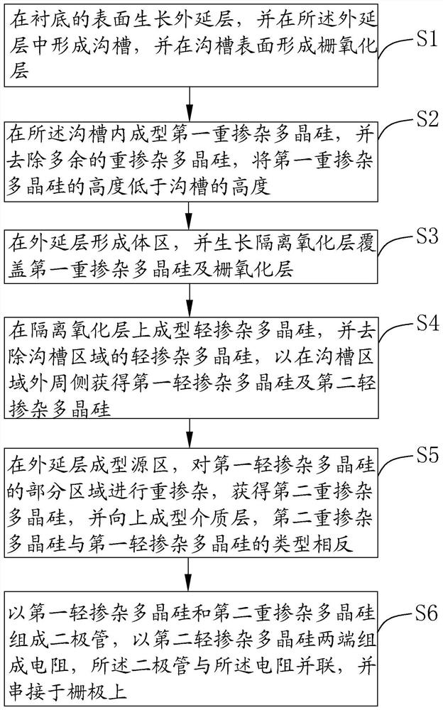
[0057] Specifically, the second heavily doped polysilicon 8.1 is implanted with boron atoms, or injected with ion implantation.

[0059] It can be understood that in step S6, holes are drilled through the first lightly doped polysilicon 8.2 and the second heavily doped polysilicon 8.1

[0061] Step S21: depositing initial polysilicon on the surface of the gate oxide layer in the trench region.

[0063] Step S23: using a dry etching process method to etch the first heavily doped polysilicon from top to bottom.

[0069] Step S63: forming a first metal connection line and a second metal connection line in the resistance contact hole, and the source region contacts

[0070] Step S64: forming a fourth metal connection and ...


PUM


Abstract

The invention discloses a MOSFET chip manufacturing method for improving gate characteristics, including forming lightly doped polysilicon on the isolation oxide layer, and removing the lightly doped polysilicon in the groove area, so as to obtain the first light Doped polysilicon and the second lightly doped polysilicon, in the source region of the epitaxial layer, heavily doped a part of the first lightly doped polysilicon to obtain the second heavily doped polysilicon, and formed a dielectric layer upwards, the second heavily doped polysilicon The type of doped polysilicon is opposite to that of the first lightly doped polysilicon, and the first lightly doped polysilicon and the second heavily doped polysilicon form a diode, and the two ends of the second lightly doped polysilicon form a resistor, the diode and the The resistors are connected in parallel and connected in series with the grid. The polysilicon resistor and polysilicon diode are integrated inside the chip, which can effectively limit the current flowing through the gate, so as to realize the protection of the gate.

Description

A MOSFET chip manufacturing method with improved gate characteristics technical field The present invention relates to semiconductor technology field, relate in particular to a kind of MOSFET chip manufacturing method that improves gate characteristic Law. Background technique MOSFET chip is a kind of discrete device, belongs to the category of semiconductor power device, and belongs to semiconductor with integrated circuit. In the field of bulk chips, integrated circuits integrate thousands of transistors into the same chip through process methods, MOSFETs It is a single transistor composed of thousands of cells of the same structure juxtaposed. [0003] The key index parameters of MOSFET include breakdown voltage (specifically drain-source breakdown voltage), on-resistance, threshold voltage and avalanche current, in general, the larger the breakdown voltage and avalanche current, the better, and the smaller the on-resistance, the better. to achieve its goal The...

Claims


Application Information

Patent Timeline
Patent Type & Authority Patents(China)
IPC IPC(8): H01L21/336H01L29/06H01L29/78
CPCH01L29/66568H01L29/7827H01L29/0603
Inventor 潘光燃胡瞳腾
Owner 深圳市芯电元科技有限公司
Why Eureka
Try Eureka