4*4 optical switch array based on organic-inorganic hybrid integration
An optical switch array and hybrid integration technology, applied in the field of optical communication, to achieve the effects of reducing process cost, improving waveguide morphology, and reducing process complexity
- Summary
- Abstract
- Description
- Claims
- Application Information
AI Technical Summary
Problems solved by technology
Method used
Image
Examples
Embodiment 1
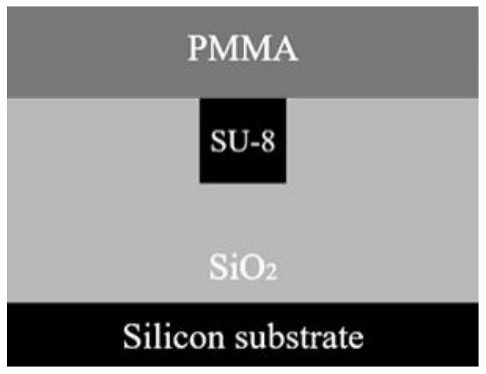
[0055] Thermal oxidation was performed on the Si substrate to grow a layer of SiO with a thickness of 5 μm 2 as the lower cladding;
[0056] to SiO 2 The lower cladding layer is etched by ICP, and the top view is the designed 4×4 optical switch array device, and the groove structure with an etching width and etching depth of 2.5 μm (the structure of the 4×4 optical switch array that is attached Figure 9 The structure formed by "cascading 5 groups of 2×2 switching units designed above" as shown can be manufactured by Henan Shijia Photon Technology Co., Ltd.);
[0057] The waveguide core material SU-8 2002 is spin-coated on the groove structure, the spin coating speed is 5000r / min, after filling the groove structure with a depth of 2.5μm, the core material will be on the top of the core layer and not etched SiO 2 A layer with a thickness of about 2.0 μm overflows from the plane where the lower cladding is located;
[0058] After spin-coating the core layer, perform pre-bak...
PUM
| Property | Measurement | Unit |
|---|---|---|
| Thickness | aaaaa | aaaaa |
Abstract
Description
Claims
Application Information
 - R&D
- Intellectual Property
- Life Sciences
- Materials
- Tech Scout
- Unparalleled Data Quality
- Higher Quality Content
- 60% Fewer Hallucinations
Browse by: Latest US Patents, China's latest patents, Technical Efficacy Thesaurus, Application Domain, Technology Topic, Popular Technical Reports.
© 2025 PatSnap. All rights reserved.Legal|Privacy policy|Modern Slavery Act Transparency Statement|Sitemap|About US| Contact US: help@patsnap.com


