MicroLED display panel and forming method thereof

A display panel and chip unit technology, which is applied to electrical components, electrical solid devices, circuits, etc., can solve the problems of unsatisfactory light extraction efficiency, poor optical matching, and light extraction efficiency of the display panel, etc. Extraction efficiency, improved light extraction efficiency, good optical matching effect

Active Publication Date: 2021-10-19
HUA WEI SEMICONDUCTOR (SHANGAHAI) CO LTD
View PDF6 Cites 1 Cited by
  • Summary
  • Abstract
  • Description
  • Claims
  • Application Information

AI Technical Summary

Problems solved by technology

[0003] The optical matching of the current Micro LED display panel is not good, the light extraction efficiency of the display panel is not ideal, and the light extraction efficiency needs to be further improved

Method used


Image

  • MicroLED display panel and forming method thereof
  • MicroLED display panel and forming method thereof
  • MicroLED display panel and forming method thereof

Examples


Embodiment Construction

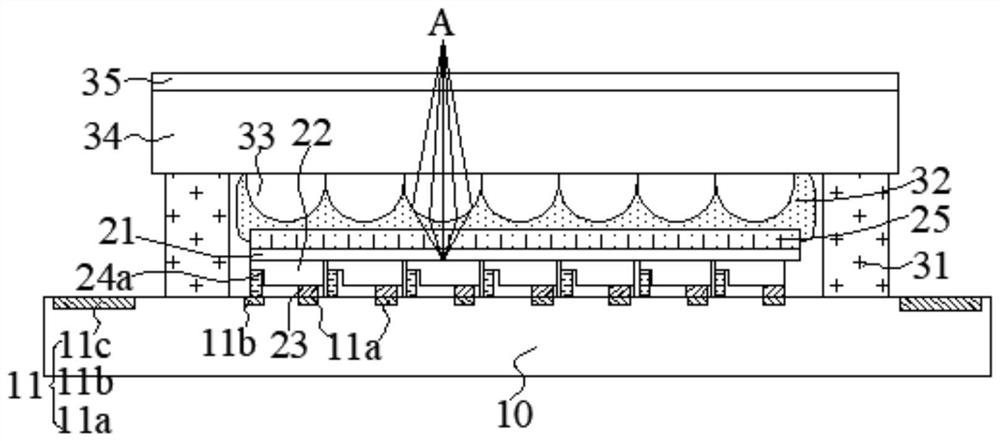
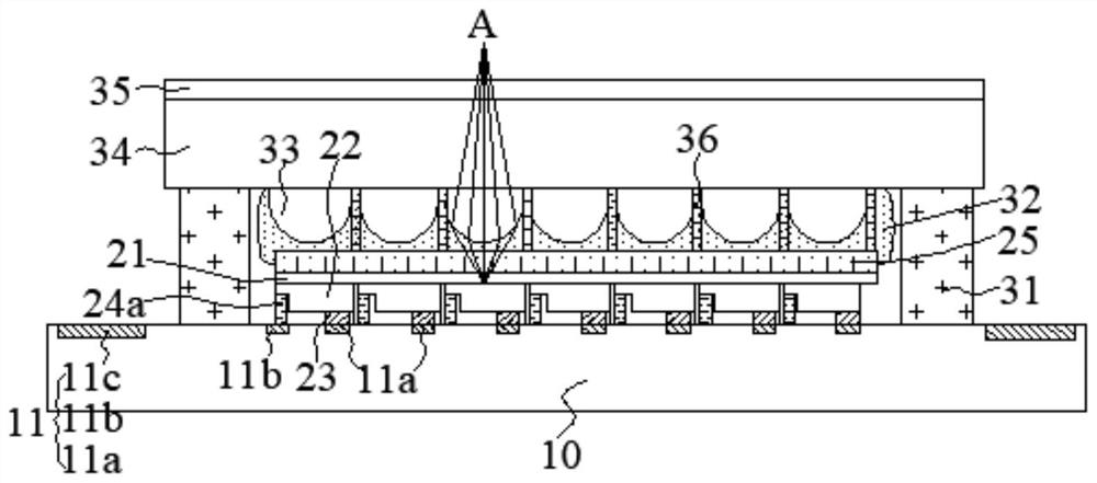
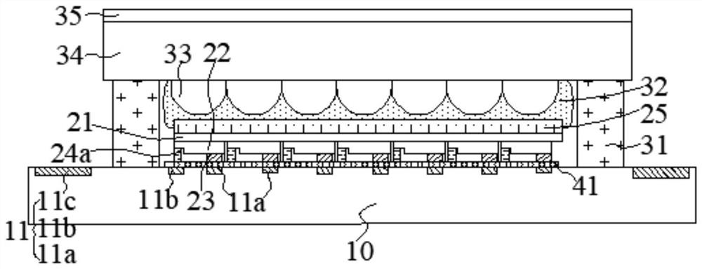
[0036] Based on the above research, embodiments of the present invention provide a Micro LED display panel and a method for forming the same. The present invention will be described in further detail below in conjunction with the accompanying drawings and specific embodiments. The advantages and features of the present invention will become clearer from the following description. It should be noted that the drawings are all in a very simplified form and use imprecise scales, and are only used to facilitate and clearly assist the purpose of illustrating the embodiments of the present invention.

[0037] An embodiment of the present invention provides a MicroLED display panel, including: a driving wafer, a MicroLED chip unit, and a microlens array; the driving wafer is bonded to the MicroLED chip unit; the microlens array includes array-distributed micro A lens, the micro-lens is in a hemispherical shape, and one side of the spherical surface of the micro-lens faces the Micro L...


PUM

PropertyMeasurementUnit
thicknessaaaaaaaaaa
thicknessaaaaaaaaaa
thicknessaaaaaaaaaa

Abstract

The invention provides a MicroLED display panel and a forming method thereof. The display panel comprises a driving wafer, a MicroLED chip unit and a micro lens array, wherein the driving wafer is bonded with the MicroLED chip unit, the micro lens array comprises micro lenses which are distributed in an array, the micro lenses are hemispherical, and one side of the spherical surface of each micro lens faces the MicroLED chip unit. Therefore, light beams emitted by the MicroLED chip unit irradiate the spherical surface of the micro lens and are converged after being refracted, and better optical matching between the MicroLED chip unit and the micro lens array is realized, so that the light extraction efficiency is improved, the focusing of emergent light rays is more concentrated, the image display is clearer, and the light extraction efficiency is improved.

Description

technical field [0001] The invention belongs to the technical field of integrated circuit manufacturing, and in particular relates to a Micro LED display panel and a forming method thereof. Background technique [0002] Micro LED (Micro light emitting diode) display is a next-generation display technology emerging after liquid crystal display and OLED display. Micro LED displays use LED light-emitting chips (Micro LED chips) with a size ranging from a few microns to tens of microns as pixel units, which are closely arranged in an array, and each chip can be independently driven to light up and emit light. MicroLEDs (also known as MicroLEDs, mLEDs or μLEDs). [0003] The optical matching of the current Micro LED display panel is not good, the light extraction efficiency of the display panel is not ideal, and the light extraction efficiency needs to be further improved. Contents of the invention [0004] The purpose of the present invention is to provide a MicroLED display...

Claims


Application Information

Patent Timeline
Patent Type & Authority Applications(China)
IPC IPC(8): H01L25/075H01L27/15H01L33/48H01L33/58
CPCH01L25/0753H01L27/156H01L33/48H01L33/58H01L2933/0033H01L2933/0058
Inventor 范纯圣范世伦
Owner HUA WEI SEMICONDUCTOR (SHANGAHAI) CO LTD
Why Eureka
Try Eureka