Method for preparing a semiconductor structure and semiconductor growth equipment
A semiconductor and equipment technology, which is applied in the direction of metal material coating process, coating, gaseous chemical plating, etc., can solve the problem of poor steepness of the growth interface, etc., and achieve the effect of eliminating dwell and improving the steepness of the interface
- Summary
- Abstract
- Description
- Claims
- Application Information
AI Technical Summary
Problems solved by technology
Method used
Image
Examples
Embodiment 1
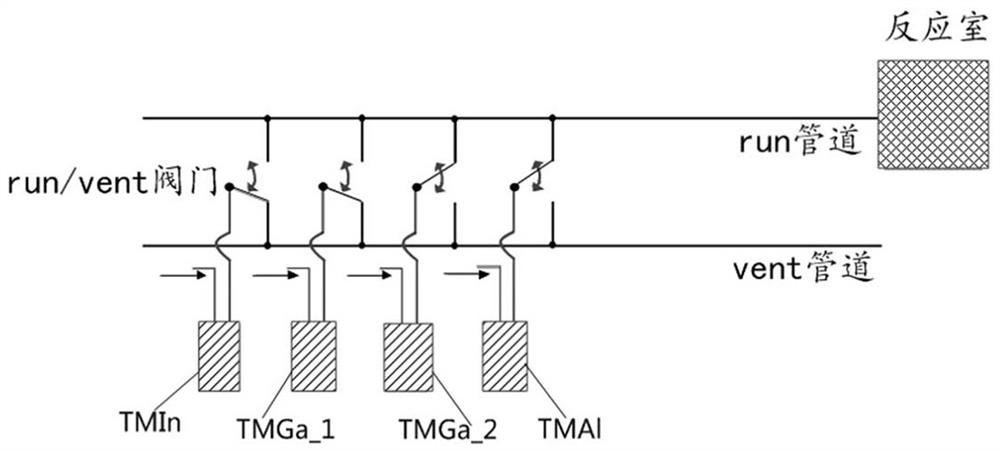
[0040] An embodiment of the present invention provides a semiconductor growth equipment, comprising:
[0041] reaction chamber 100;
[0042] a main growth pipeline 110, one end of the main growth pipeline 110 is connected to the reaction chamber 100;
[0043] Vent the main pipeline 120;
[0044] From the first mixing main pipeline to the Mth mixing main pipeline, M is an integer greater than or equal to 1;
[0045] The first reaction gas source group to the Nth reaction gas source group, N is an integer greater than or equal to 2;
[0046] From the first switching valve group to the Nth switching valve group, the kth switching valve group is suitable for controlling the transmission of the gas in the kth reaction gas source group to the jth mixing main pipeline; k is an integer greater than or equal to 1 and less than or equal to N; j is an integer greater than or equal to 1 and less than or equal to M;
[0047] The first growth and vent switching valve to the Mth growth a...
Embodiment 2
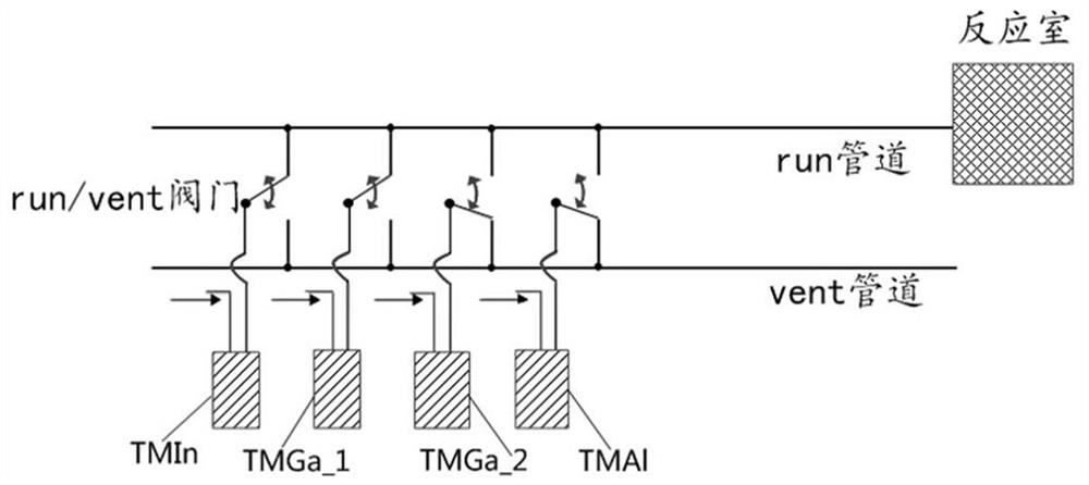
[0067] The difference between this embodiment and the previous embodiment is: M is greater than or equal to 2, and M is less than or equal to N, and the kth switching valve group is suitable for switching the gas in the kth reaction gas source group to the jth mixing main pipeline or to the jth mixing main pipeline. Vent the main transmission line.
[0068] The k-th reaction gas source group includes several k-th sub-reaction gas sources, specifically, the k-th reaction gas source group includes Q k The kth reaction gas source, Q k The k-th sub-reaction gas source is respectively the first k-th sub-reaction gas source to the Q-th sub-reaction gas source k The kth sub-reaction gas source. Q k The gas in the kth sub-reaction gas source is different. Q k is an integer greater than or equal to 2. The gases in several kth sub-reaction gas sources are different.
[0069] The k-th switching valve group includes several k-th sub-switching valves, specifically, the k-th switchin...
Embodiment 3
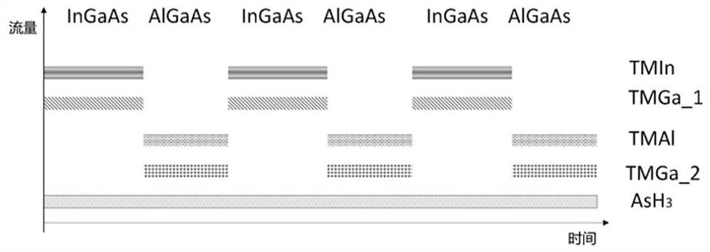
[0081] This embodiment provides a method for preparing a semiconductor structure, using the above-mentioned semiconductor growth equipment, including the following steps:
[0082] Step S1: the kth 1 Switching valve group controls the kth 1 The gas in the reaction gas source group goes to the jth 1 Hybrid Main Pipeline, Section J 1 kth in the mixing supervisor 1 Reactive gas mixture; k 1 is an integer greater than or equal to 1 and less than or equal to N;
[0083] Step S2: the jth 1 Growth vent switching valve switching jth 1 The kth in the mix main pipeline 1 The reaction mixture gas is transported to the growth main pipeline;
[0084] Step S3: the jth 1 Growth vent switching valve switching jth 1 The kth in the mix main pipeline 1 After the reaction mixture gas is transported to the main growth pipeline, the first growth vent switch valve to the Mth growth vent switch valve are all switched to communicate with the vent main pipeline so that the growth interruption...
PUM
 Abstract
Description
Claims
Application Information
 - R&D Engineer
- R&D Manager
- IP Professional
- Industry Leading Data Capabilities
- Powerful AI technology
- Patent DNA Extraction
Browse by: Latest US Patents, China's latest patents, Technical Efficacy Thesaurus, Application Domain, Technology Topic, Popular Technical Reports.
© 2024 PatSnap. All rights reserved.Legal|Privacy policy|Modern Slavery Act Transparency Statement|Sitemap|About US| Contact US: help@patsnap.com


